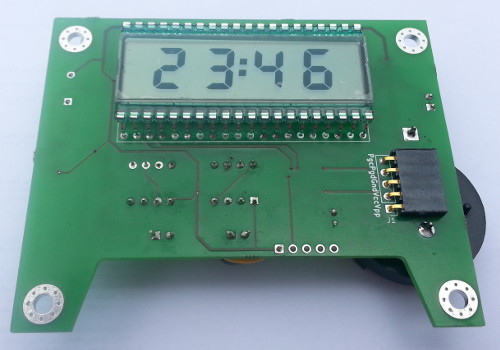
LCD timer, 2nd gen.
03 August 2020This is a complete redo of my LCD timer, this time designing the PCBs to fit the mounting studs available on the Hammond Manufacturing
1591XXS enclosure.
Unlike the previous timer which was built in mostly-independent stages, this one is built as an integrated effort using a single PCB for all circuitry that was previously split between two boards.
This article covers creation of the circuit itself, whereas a future article will detail the enclosure itself, including how it was selected and the circuitry mounted.
This project has been ongoing since summer last year and by any measure has been drawn out and troubled. False starts, design error & fabrication flaws that rendered boards salvageable, and various outside factors that delayed getting things done. As a result this article is not a complete telling of the story behind the PCB.
Background to making LCD timers
These days I find many of the electronics articles I wrote back in 2017 to be cringeworthy, but had it not been for my overly-verbose writing about things like the difference between the various timers available on PIC microcontrollers, I likely would have long forgotten what I did and when. Time-keeping — much like LED control — is something I rehashed a bit too much, to the extent that I forgot how many circuits I had built. In hindsight the relevant mile-stones were figuring out how to use timers in the first place, working out how to wire an external crystal, developing de-bouncing logic, and finally figuring out LCD display drivers. When I was originally sourcing an LCD display I always intended it to be used as part of a timer circuit, but it turned into an incremental process due to the number of mile-stones involved — these fell into roughly three parts:-- Experimentation
- The first stage was understanding how LCD displays worked and the specifications of the driver chip that a display needed, which was the end result of the effort that went into LCD display & driver. I realised that rather than being able to wire up an LCD panel the same way I could test an LED module, LCD displays require AC signals that came with their own nomenclature. However this was in parallel with the task of finding an LCD panel that had the segment layout suitable for time display, which was just one of many challenges.
- Packaging
- The next stage was turning the experimental circuit into a self-contained PCB that would be used as a daughter-board with minimal connections. Difficulty with routing all the tracks made me use it as an excuse to see what designing a four-layer PCB would be like, which I have no regrets about even though I now know that two layers were sufficient. Main realisation is that laying out tracks is more of an art than a science.
- Practical use
- After a long delay I finally got round to building a timer that used the LCD display daughter-board, which in turn was based on a prior LED-based timer — the latter separated timing and display control which communicated via I2C, so only the content of the I2C update commands needed updating. Initially prototyped using perf-board it was later converted into a PCB, but unfortunately it was botched. After some rework I did finally build the enclosed timer I had long-intended.
Circuit design & implementation
The circuit itself is schematically a combined and corrected version of the two-board design the previous timer used, with some extras based on perf-board prototyping, and with the physical dimensions of the board itself made to fit a specific enclosure. This process was far from smooth but I felt it better if this article did not catalogue all the mis-starts and outright mistakes; therefore the following sub-sections will detail the various parts of the working revision of the combined circuit, with some background of how they came about.
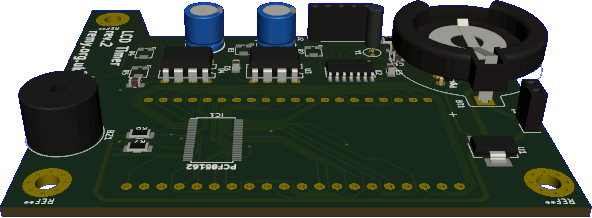
LCD panel & driver sub-circuit
The LumexLCD-S401C39TR — shown below — and NXP PCF85162 combination of LCD driver and display is one that I experimented with and then turned into a self-contained component, although the latter process was quite a major effort given the number of connections required. Before designing the rest of the circuit I just included the LCD dispay and driver chip, because I knew that most of the trouble would be connecting these two things together, and it would also be an easy place to make a mistake — in fact there was a mislabelling on one of my KiCad schematic symbols, which I missed because I wired up everything based on pin numbers instead.
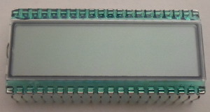
Looking back at my original experimental try-out article the circuit wiring table was very useful as it mostly negated the need to trawl through data-sheets, aside from a few spot-checks in places I felt a mistake was possible, but it was from the perspective of the LCD display which made checking driver pin connections a bit difficult. The table below gives the pin connections for the PCF85162 itself, together with an overview of what is connected to them.
The only pin I would consider changing is SA0 which chooses between one of two I2C addresses. The pins A0 thru A2 use some contrived mechanism that allows multiple drivers to use the same I2C address, which to me seems close to abuse of the I2C specification.
| Conn. | 3D | 3E | 3G | 3F | 3A | 3B | x3C | D.2 | 2D | 2E | 2G | 2F | 2A | 2B | 2C | D.1 | 1D | 1E | 1G | 1F | 1A | 1B | 1C | n/c |
| Pin label | S48 | S47 | S46 | S45 | S44 | S43 | S42 | S41 | S40 | S39 | S38 | S37 | S36 | S35 | S34 | S33 | S32 | S31 | S30 | S29 | S28 | S27 | S26 | B4 |
| Pin number |
48 | 47 | 46 | 45 | 44 | 43 | 42 | 41 | 40 | 39 | 38 | 37 | 36 | 35 | 34 | 33 | 32 | 31 | 30 | 29 | 28 | 27 | 26 | 25 |
| 1 | 2 | 3 | 4 | 5 | 6 | 7 | 8 | 9 | 10 | 11 | 12 | 13 | 14 | 15 | 16 | 17 | 18 | 19 | 20 | 21 | 22 | 23 | 24 | |
| Pin label | S23 | S24 | S25 | S26 | S27 | S28 | S29 | S30 | S31 | SDA | SCL | Sync | Clk | Vdd | Osc | A0 | A1 | A2 | SA0 | Vss | Vlcd | BP0 | BP1 | BP2 |
| Conn. | D.3 | 4C | 4B | 4A | 4F | 4G | 4E | 4D | : | I2C | n/c | Vcc | Ground | Vdd | C | n/c | ||||||||
When I was designing the stand-alone LCD time-display PCB I had trouble with the number of tracks that needed to cross, and I ended up making it a four-layer PCB rather than the usual two-layer. In itself I have no regrets about making it a four-layer but having laid out the connections again from scratch, it is now clear that a fundamental mistake I made was having the driver chip horizontal rather than vertical. Rather than crossing the wires needed to be attached to the driver pads underneath the chip, they are routed out the ends and around the wires that are attached from the outside — this is most obvious just off the bottom-left corner of the driver chip in the cross-section rendering below.
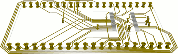
Previously I would have avoided putting tracks between mounting holes and for space reasons I wanted all tracks to be between the two rows, but this would have just meant using a lot more vias. This time round I specifically tried to minimise vias, as this was intended to be part of a much larger PCB, and I think getting it down to six was good going — the extra four to the right are place-holders, since the rendering was made before the rest of the circuit was laid out. I later managed to remove the three vias that are below the driver chip.
Timer control circuit
The main control sub-circuit is essentially a MicrochipPIC16F1823 wired up with a Abracon AB38T crystal, which for me is a tried-and-tested combination — the only change from the previous control circuit is the use of surface-mounted capacitors instead of through-hole ones. I kept the same pin wirings so that the firmware from the previous timer could be reused with few if any modifications, and these connections are shown in the schematic fragment below.
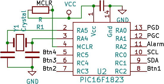
I originally decided to rely on a programming clip to flash the PIC16F1823 and reuse the adapter I built previously, but when I had to redesign the circuit due to faults I decided to add a dedicated flashing header to the second revision. A problem with programming clips is that sometimes it is hard to get a good connection.
Sounder circuit
Finding a sounder with the right tone, physical size, and voltage requirements, has proven to be a headache. The PIC16F88 LED alarm clock — one of many LED-based timing circuits made in a short period of time, hence the rather detailed title — included a working sounder but since it required an 8-15 volt upply the sounder was connected directly to the unregulated 9-volt power supply and controlled by an NPN transistor on its ground connection. The only sounders I found that were both physically small and required a low voltage were ones that are basically mini speakers that have to be driven by an alternating signal, the duty cycle and period of which controls the tone.
I eventually built a proof-of-concept driving circuit that used two 555 oscillators — one to control the pitch, and one to control the on and off periods of sound. This approach was used as-is and is shown in the schematic below — the output of the second 555 drives a Pro-Signal (now part of Multicomp) ABT-414-RC sounder via a Sziklai pair of transistors, although the latter is not shown.
While it is possible that one or both 555s could be omitted and the task instead done in firmware, the hardware solution provides more intuitive control over how the alarm sounds, and allows the same firmware from the previous timer to be re-used unmodified.
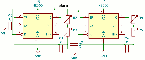
For some reason at the time of designing the circuit the NE555P was only easily found in DIP form, and I usually avoid through-hole components for PCBs due to them taking up space on both sides of the board. Because the NE555P at least in theory requires at least 4.5 volts I switched to the LMC555 which is a pin-compatible variant that needs only 2 volts.
For the second board revision I also added provision for a grounding capacitor to the CV pins rather than leaving them floating, as well as bypass capacitors.
Power supply
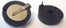
As with the previous timer, a double-stack of 3 volt button batteries within a Keystone1025 — shown below — feeds a 3.3 volt power regulator. I would prefer to have used a 5 volt regulator, but such regulators typically need an input voltage significantly more than 6 volts. The regulator I used was a Texas Instruments UA78M33CDCYR which apparently has been discontinued by Farnell, but I had bought a large stock of them while they were still available.
Circuit design faults
I sent a first revision of the PCB off for fabrication in November 2019 and unfortunately it was affected by an embarrassing number of flaws, so I eventually had a second revision of the PCB fabricated. The individual flaws are detailed below and while it may have been possible to rework around them I decided that doing so would be too much trouble. This was not an easy decision to make given that I had made a special effort to get the board complete by the end of that year.- Incorrect PCB markings
- For some reason the PCB markings had “ARM” even though this is really PIC-based, and I can only speculate as to why I put in this incorrect text. A somewhat careless cosmetic error that may be due to having designed and ordered for fabrication other ARM PCBs around the same time.
- Incorrect Sziklai pair wiring
- The Sziklai pair that powers the sounder had the collector and emitter of the PNP transistor the wrong way round in the schematic. It is possible this was taking account of a pin-flip on the PCB foot-print, but due to differences between pin numbers in KiCad versus the transistor data-sheets I ended up deleting and redoing this part of the circuit from scratch.
- Missing I2C pull-ups
- During development I switched between having a single PCB and a two-board design, and I suspect somewhere along the line the I2C pull-up resistors got omitted when I recombined the schematics into a single circuit. However omitting pull-ups is a mistake I have made more times that I want to admit, not helped because for testing purposes I often in the past used I2C devices with a master that had them built-in.
- Components too close together
- The proximity of the microcontroller to one of the 555 trimmers meant that I was not able to securely attach the programming clip. At first I thought it was due to excess solder causing a poor grip, but after many cleaning attempts I notice the clip banging into the trimmer. This is the fault that made me abandon the PCB and do a redesign.
- 555 oscillators wrong way round
- The two 555 chips in the sounder circuit had the wrong capacitor footprints, which was a problem as 220μF is not available in SMD size 0805. I only noticed this one later when recycling the board for lead-free solder testing and it is just as well I held back ordering in the revised PCB.
Circuit production
Although this was not the only PCB I designed in 2019 it was by far the most complex — the bi-directional RF board was based on a reference design and was actually laid out back in 2018 — and partly because of this it was a long time in the making. As detailed above it had a rather troubled production that meant it went through two revisions. The next sub-sections cover the details of the physical building of the circuit.PCB fabrication
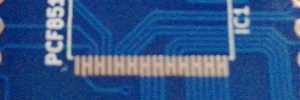
For this circuit I used Seeedstudio since unlike the other two fabrication services I use they charge pretty much a flat rate for PCBs where both dimensions are under 10cm, in this case the overall cost being $25 for 10 boards including delivery. Since this is a circuit I might give to other people once completed I opted for the HASL lead-free finish rather than my usual lead-based finish, and used lead-free solder when mounting the components — I normally use lead-based solder so most of the time I see no advantage in getting lead-free PCBs, but this one was to be an exception. Having not used lead-free solder since my earliest circuits back in 2017 I felt it was time to see how it really performed compared to lead solder.As it turned out when Seedstudio fabricated the second revision of the board there was a serious manufacturing flaw. Several pins were bridged together that should not have been, as shown in the picture below, and this rendered the PCB useless. Had I noticed this back in March when I received the order I would have asked them to do the job properly, but since I did not unpack the PCB until July it was a bit late to demand that. I downloaded the Gerber files attached to the order in my Seeedstudio account and they looked fine — I actually submitted this zipfile unchanged to Aisler who went on the fabricate the board properly.
I suspect this error is deliberate sabotage by a disgruntled employee, because it does not look like the sort of thing that would be caused by a simple slip, and in the past Seeedstudio have spotted and corrected mistakes on my part. Either way I was obviously disinclined to trust Seeedstudio with the respin, especially with a 3-5 week turnaround time.
Component sourcing
Below is a list of the major components used to populate the circuit, together with part numbers and vendor stock codes. All the components required for this circuit were ones I had left-over stock of from previous projects, which includes components that I stocked well over a year ago and in cases have actually been discontinued by the vendor I got them from. I have omitted unit prices as in most cases they will have changed.
| Description | Manufacturer | Part number | Vendor | Order code |
| Microcontroller | Microchip | PIC16F1823 |
Farnell | 2308690 |
| 32.768kHz crystal | Abracon | AB38T |
1611828 | |
| LCD display | Lumex | LCD-S401C39TR |
Digi-Key | 67-1792-ND |
| Mouser | 696-LCD-S401C39TR | |||
| LCD driver | NXP | PCF85162 |
Digi-key | 568-5059-1-ND |
| Mouser | 771-PCF85162T/1118 | |||
| 555 Oscillator | Texas Instruments | LMC555CN |
Farnell | 9488243 |
| Sounder | Multicomp | ABT-414-RC |
2098836 | |
| 0.1μF (100pF) capacitor | Kemet | C322C104K5R5TA7301 |
2575663 | |
| 220μF capacitor | Multicomp | MCGPR10V227M6.3X11 |
1902883 | |
| PNP 22k/47k Transistor | Nexperia | PDTC124XU,115 |
8737215 | |
| NPN 100k/100k Transistor | ROHM | DTC115ECAHZGT116 |
2769605 | |
| Trimmer | Panasonic | EVM3YSX50B14 |
discontinued | |
| Voltage regulator | Texas Instruments | 2205061-1 |
discontinued |
The LCD display and drivers were from an existing stock I bought over from the US via Digi-Key back in early-2018 but I found out they are also available from Mouser without having to pay the import duties — I am guessing it is cheaper for them to pay the duties than to actually have a warehouse in Europe. I am not sure if Mouser have the same range as Digi-Key but Mouser is now my go-to vendor for stuff that Farnell do not stock.
Component soldering
Although I normally prefer to hand-solder even quite small surface-mount components, I felt that the 48-pin TSSOP LCD driver chip was best reflow-soldered. The amount of flux I needed to hand-solder SSOP chips on my ARM-based I2C master was fresh in my mind, so the messiness of solder paste seemed a small price to pay — the tin-bismuth pastes I use are already lead-free and in practice I have found rework to remove any solder bridges easy-going due to its low melting point. For the first revision I reflowed just this chip using the same stencil that I used for the stand-alone LCD display PCB, but for the second revision I got a custom stencil for the whole PCB and reflowed all the surface-mounted components. I did this because I had awful experiences with the first revision trying to hand-solder with lead-free solder wire although this was basically down to a poor choice of solder wire.Post-reflow rework
As is often the case with reflow soldering there were bridges that needed to remove. Sometimes bridges just need a clean soldering iron to sweep away but most of the time some flux is also needed, and this time round I used MG Chemicals8341-10ML flux paste. This paste is a viscous flux dispensed via a syringe which seems popular with people on YouTube so decided to give it a try.
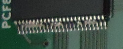
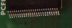
For large bridges such as the ones shown in the first picture below some solder wick is needed to soak up the excess solder, and the second picture below shows the chip after all the bridges are gone.
I am not sure how the flux paste compares to the flux pen I have used a lot in the past, but it does at least have the advantage in that it does not start flowing away until a soldering iron is applied. Bridge-removing rework is a bit of an art, sometimes with bridges lifting up easily and at other times remaining stubborn. The soldering iron was brand new so I suspect being very clean was a factor.