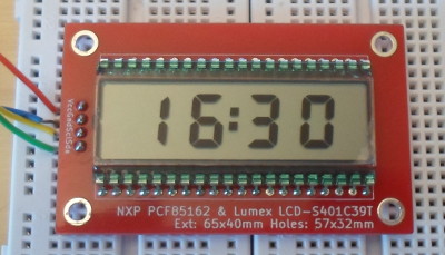
LCD time display PCB
26 April 2018This printed circuit board is an LCD time panel and an LCD driver chip combined, making a componentisation of the experimental LCD display & driver I built last month on solderless breadboard. I have created daughterboards in the past, most notably the matrix modules used on the column driver boards within my LED matrix display, but this board is the first that is intended to be generic rather than for use in a specific project.
The driver commands are the same as in the prototype, and having the PCB component lets me reclaim the breadboard & wires.
Board design
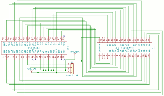
The circuit design is basically the testing setup I had used previously, with the voltage regulator and USB I2C master replaced with a pin header, and the eeschema schematic is shown below. The amount of crossing-over wires reflects the messiness of the original solderless breadboard, and this will cause plenty of pain in the laying out of the PCB.
PCB footprints
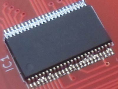
For some reason the stock TSSOP-48 footprintHousings_SSOP:TSSOP-48_6.1x12.5mm_Pitch0.5mm had 1mm long pads, whereas the PCF85162 data-sheet recommends 1.4mm pads, which is not the first time I have had issues with KiCad footprints being a bit too short. It was simple enough to make a copy of the footprint and modify the pad lengths, after which the footprint matched the data-sheet perfectly, although I found it easier to edit the .kicad_mod footprint files directly with a text editor rather than change all the sizes within the KiCad PCB footprint editor. For the Lumex LCD panel I had to make a footprint from scratch, but it was easy enough as it was basically two rows of through-hole mountings, although once again it was easier to create the pads (i.e. the holes) within the footprint editor, and then edit the locations using a text editor. I was not aware of a 3D model for the LCD panel, and was not in the mood to work out how to create my own, so I had to omit including one.
I remember reading in the Hackaday guide that creating custom component footprints is actually a standard part of PCB design, and so far I am inclined to believe this. For PCBs I expect at the very least to have to modify any stock footprints, and in hindsight for the PIC16F88 Timer PCB should have made some of the component though-hole pads that bit larger. I gave up on Fritzing because its range of SMD footprints was deficient — although to be fair the footprints it did have turned out to be good fits — and trying to make custom ones looked like an ordeal I never followed through with.
Routing the tracks
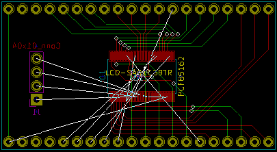
Routing the wires for this PCB was a complete nightmare, due to the number of tracks that cross over each other. Rather than putting the driver chip directly below the LCD panel, I had intended to put it on the other side of the PCB, but that made the crossing-overs even worse. I had also intended to use only two copper layers and this attempt is shown below, but in the end I concluded that it was not possible to wire up all the pins, at least not without a lot of hopping between layers to deal with crossed tracks.
In the end I decided to use four copper layers, which actually turned out to be not much more difficult than working with two layers. Only new thing was using < (shift-dot) in order to choose which layer to switch to, rather than v that previously toggled between the top and bottom copper layers. However even with four layers it turned out to still be a squeeze to get all the pins routed. The result is shown below, and it is less pretty than I would have liked, but after having to constantly delete and reroute existing tracks I concluded the result was never going to look pretty.
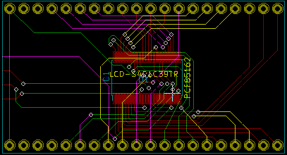
In hindsight there was not really the space available for a proper fan-out of the TSSOP pins, and in particular I am not exactly happy with the amount of tracks & vias underneath the driver chip itself, but as has been the case in the past other things have dictated the space available. For this PCB I avoided the use of blind & buried vias, which are vias that do not connect all of the copper layers, because I felt that they would be more trouble than they are worth. In any case I thought that going from two to four copper layers was enough to worry about.
Adding the mounting holes
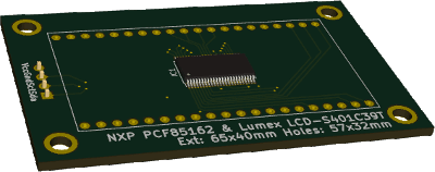
I felt that the mounting holes on the 16F88 Timer PCB were a little skimpy, which was in part due to the limited space available for them. They were that bit too tight for the self-tapping bolts (Farnell 2474995) I used, and they did not really have a proper flange for the bolt to grip. This time round I decided to be a lot more generous, using a diameter of 3.3mm and having a proper grip area of 5mm, with the size of the board being made to accommodate the size of bolt-holes rather than the other way round. The 3D model of the complete PCB is shown below:
In hindsight I wanted to have used the stock Mounting_Holes:MountingHole_3.2mm_M3_Pad_Via rather than making my own mounting holes, but I doubt this is a big deal in practice. I suspect the supposed extra reinforcement is in practice cosmetic, and claearance between where the bolt grips and elsewhere is already ample.
Blind & buried vias
With 2-layer PCBs all vias are through-hole vias, which pass through the entire PCB, bit with 4+ copper layers there are blind and buried vias that only pass between some of these layers — the difference between buried and blind being whether one of these layers if the top or bottom (i.e. external) layer. From the start I decided not to deal with blind & buried vias, mainly because I had recollections about them not being widely supported by fabrication services, so felt there was little point in adding the complexity of thinking about them. For me worrying about four layers of signal tracks rather than two was enough extra stuff to worry about.As things turned out of the 33 vias in the final PCB layout, only 3 were not connected to the top copper layer, and 2 of these were well away from the foot-print of the LCD driver chip — as a result blind & buried vias simply would have not offered any practical flexibility. In addition OSH Park does not support them at all, Aisler does not state anything about it, and ticking the option for them on the Seeed Studio quote page increased the cost from $43.11 to $469.77 — from what I can tell the problem is having multiple drill layers, because it means drilling & plating has to be done on a layer-by-layer basis, whereas with a single drill layer such penetrations are done once everything has already been sandwiched together.
Fabrication quotes
Even though from the start I planned to use Seeed Studio, I thought it only fair to get quotes from the other two PCB fabrication services I have used in the past, and the prices are shown below. Seeed Studio offer both lead and lead-free PCBs, but I decided to pay the extra $7 for the lead-free option simply to avoid any potential importation issues.- Aisler
- €14.30 per PCB (multiples of three)
- €12.80 for solder stencil
- Free shipping
- Total: €42.90
- €12.80 for solder stencil
- OSH Park
- Three PCBs
- Solder stencils not offered
- Free shipping
- Total: $40.50 (€32.65)
- Solder stencils not offered
- Seeed Studio
- $43.11 for 10 PCB ($4.70 discount)
- $8.90 for solder stencil
- $15.97 EU Post shipping (10-18 days)
- Total: $67.98 (€54.80)
- $8.90 for solder stencil
Reflowing & populating
For this PCB I broke out the Chip Quik solder paste (Digi-Key SMDLTLFP-ND; Farnell no longer stock), which has substantially lower operating temperatures than the solder paste I have used in the past — this was why I screwed up the first PCB, as I nudged the chip before the solder joints had solidified. The paste itself was also noticeably less viscous than my previous paste, which I suspect resulted in more solder bridges, but removing the solder bridges was also a lot easier due to the much lower melting temperature. Clearly a higher-quality paste, but for now I am unsure whether the 5-fold higher price is justified.
I decided that I did not want the LCD panel resting directly on top of the driver chip, so I used some blu-tack to hold it a bit above while I soldered the four corner pins. I had tried to test the PCB without soldering the LCD panel in place, but the results I got trying to do this were somewhat non-conclusive, so I decided to just go ahead and solder the panel into place. As it happened it just worked without any problems.