PIC16F88 8-segment LED timer
28 January 2018This circuit is the previous 8-segment LED timer rebuilt to use a
PIC16F88 instead of an I/O expander, as well as using an external clock crystal rather than relying on the internal oscillator of the PIC12F1822 for time-keeping. As a result main goals of this project are working out I2C slave functions and use of external clocking circuits, although unlike previous circuits there is also proper use of decoupling capacitors. The ultimate goal is to build a PCB timing circuit that is then installed into a box, but for this article the building of the prototype will be covered.
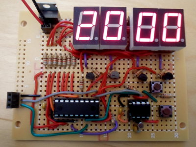
This is the third iteration of LED timing circuits, and this time round I will aim to make the article a more complete and self-contained, so knowledge of the previous iterations is not required. I have also made greater use of images to illustrate specific components. A future article will cover the building of a PCB version and the production of a box for it.
Circuit design
An overview of the circuit is show in the schematic below, which follows my usual pattern for controlling LED-based displays. Each of the segments on the LED chips is connected to a power bus from thePIC16F88, shown here with five lanes though in reality there are eight, and in turn each LED chip is switched on using a low-side NPN transistor (Farnell 2453790) that acts as a current sink for the LED chip ground pin. The NPN transistors in turn are also controlled by the PIC16F88, which receives via I2C updates from the PIC12F1822, the latter of which does the actual timing. For clarity the integrated circuit Vcc and ground connections have been ommitted.

One apparent change from the previous 7-segment display and 8-segment LED timer is that button presses are handled by the main microcontroller directly, so the PIC16F88 only does output. Having the expanders handle input as well as output was a source of all sorts of problems, and for just two buttons it is simply so much easier to have the timing microcontroller handle them directly. Below are various design decision remarks:-
- Off-loaded refresh cycle
- Because the
PIC16F88lacks the hardware to act as a I2C master I decided to use it instead of a dedicated I/O Expander in order to use up my stock of the former. However thePIC16F88is able to handle the refresh cycle itself, so incoming I2C transactions contain just the updates of the numbers to display. As a result the LED switching is off-loaded from the control loop within the main microcontroller, which seperates it from the time-keeping code. - Button pull-down
- I normally opt for button presses to be pull-up on pins with pull-down resistors, but by accident I found out that the
PIC12F1822has internal weak pull-up resistors, and they are enabled by default on pins configured for input. As a result of this finding, I switched to buttons being pull-to-ground. - Choice for main microcontroller
- I used the
PIC12F1822for the main circuit control because it was the microcontroller I selected previously and that sub-family of PIC chips are my usual choice for I2C masters. With an external clock crystal, an I2C connection, and two button inputs, all pins are in use so it makes efficent use of circuit board space. - External clock crystal
- For this iteration I decided to use an external clock crystal because the internal oscillator requires the firmware to be calibrated, which in itself is a bit of a pain to do, and even then I have doubts about its accuracy. I still use the internal oscillator for clocking the chip itself, but will use the crystal to clock Timer1.
Resistor values
ThePIC16F88 can supply 25mA per pin, but is limited to a total current draw of 100mA across all pins, which for a microcontroller is actually quite high. This translates into a per-segment power budget of 12mA, but below 30°C the forward current of the LED chip is 30mA, which implies 3.75mA per segment. I've no doubt that the LED chips can handle a lot more, as in the previous circuit they drew 43mA without problems, but this time round I decided to stick to a more conservative reading of the recomendations. The schematic below is a representation of the power path for a single LED segment, which is an updated version of the schematic I used previously to check component ratings.

Using the voltage drop of 2.53V I recorded last time, I calculated that 3.75mA would require a resistance of 750Ω, but I did not have this value in stock so instead I used 820Ω as a starting point. This drew 3.7mA which was pretty much my target current, so this is the value I went with, and I also stuck with 12kΩ for the NPN base resistance because I did not have a suitable alternative. I decided not to factor in the duty cycle, as I was undecided whether to go for the basic 25% or whether to have shorter blinks as a power-brightness trade-off. The unloaded microcontroller pins had a measured voltage of 4.86V. I also made measurements using 390Ω rather than 820Ω, but decided not to go with the resulting 6.8mA draw.
Crystal wiring
Clock crystals expect a certain capacitance, known as the load capacitance, but a complicating factor is that capacitance of the electrical paths contributes to this quantity. This contribution is known under various terms such as stray capacitance and parasitic capacitance, but the main problem with it is lack of concrete guidance about what quantity to assume, especially for through-hole components. The most informative document I found was TB097, because it gives actual capacitance values for an easily-obtained oscillator, and the implied 1.33pF stray capacitance is not far off the 2.1pF implied in AN1288. Since I don't have test equipment, ancedotal information is all that is available.
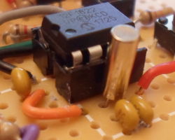
For this prototype circuit I wanted to go with 15pF capacitors which gives an allowance of 5pF for stray capacitance, working on the basis that the through-hole connections will contribute a bit towards it compared to the SMD circuit shown in TB097 mentioned above. However the closest I had to 15pF was 10pF and 22pF so I went with 22pF, and these can be seen at the bottom-right of the image above. I am convinced that despite what the PIC12F1822 data-sheet shows, a drive-limiting series resistor is required for Timer1, but I left it out because of limited space.
Decoupling capacitors
Although they are not shown in the schematic above, for this particular project I decided to include decoupling capacitors, which are capacitors placed between the Vccand ground pins of the microcontrollers in order to smooth out variances in power demand. One can be seen on the left-hand side of the pictures above and below — Vcc and ground are the orange and black wire respectively, and the capacitor connects together the power tracks close to the wire connections.
I have not bothered with them in the past as they very first time I used them one popped in front of me, and I suspect they are not really required for the circuits I tend to build, but leaving them out is not exactly good practice. Since for this circuit I intended to use an external oscillator, I decided that I ought to pay attention to signal noise reduction this time round.
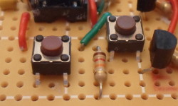
On-board buttons
For some reason nice small through-hole mounted push buttons are not stocked by Farnell or Maplin, so in the past I have used external buttons connected via a header, which is basically a pain. I eventually managed to source some from E-bay, even though these days it is not a favourite place to source electronic components due to previous trouble. From the previous timer circuits I knew that only two buttons were needed, and there was just about enough spare room to fit them.
LED control firmware
This is the firmware running on thePIC16F88, and it simply displays the time values it receives via I2C. For completeness the firmware also implements reads from the I2C master, but since read functionality is of no practical use within this circuit the reads return dummy data — it is included in this article for future reference purposes.
#define NO_BIT_DEFINES #include "pic16f88.h" __code short __at (_CONFIG1) cfg0 = _FOSC_INTOSCIO & _WDT_OFF & _MCLR_OFF & _PWRTE_OFF & _CP_OFF & _CPD_OFF & _LVP_OFF; // Mapping of bits controlling segments & chip drains unsigned char dot = 0x80; unsigned char segs[11] = { 0xcf, 0x42, 0x97, 0xd6, 0x5a, 0xfc, 0xdd, 0x4e, 0xdf, 0x5e, 0x9d }; unsigned char chips[4] = { 0x40, 0x20, 0x08, 0x04 }; unsigned char iMin = 0; unsigned char iSec = 0; unsigned char iDot = 0b0000;
void i2cSetup(void)
{
SSPCON = 0b00110110;
SSPADD = 0x02;
}
void i2cSlaveWrite(unsigned char bite)
{
SSPCON &= ~0x80;
SSPBUF = bite;
while(SSPCON & 0x80)
{
// Collision. Retry..
SSPCON &= ~0x80;
SSPBUF = bite;
}
}
void main(void)
{
unsigned char iValue = 0;
unsigned char idxChip = 0;
unsigned char iByte;
unsigned char idxWrite = 0;
unsigned char iCnt = 0;
pinSetup();
clockSetup();
i2cSetup();
while(1)
{
if( idxChip == 0 )
iValue = (iMin & 0xf0) >> 4;
else if( idxChip == 1 )
iValue = (iMin & 0x0f);
else if( idxChip == 2 )
iValue = (iSec & 0xf0) >> 4;
else
iValue = (iSec & 0x0f);
PORTB &= 0b00010010;
PORTA = segs[iValue];
if( (0b1000 >> idxChip) & iDot)
PORTB |= dot;
PORTB |= chips[idxChip];
idxChip++;
if(idxChip == 4)
idxChip = 0;
setRefreshTimeout();
while( ! (PIR1 & 1) )
{
if( PIR1 & 0x08 ) // I2C Interrupt
{
if( SSPCON & 0b1000000) // I2C Overflow
{
iByte = SSPCON;
iDot = 0b1111;
SSPCON &= ~0b1000000;
PIR1 &= ~0x08;
SSPCON |= 0b10000;
}
if(SSPSTAT & 0b100) // I2C read
{
PIR1 &= ~0x08;
if(! (SSPSTAT & 0b100000))
{
iByte = SSPBUF;
iCnt = 0;
}
else
iCnt++;
while(SSPSTAT & 0b1);
i2cSlaveWrite(0xe0 | iCnt);
SSPCON |= 0b10000;
continue;
}
while(SSPSTAT & 0b1) // I2C writes
{
iByte = SSPBUF;
if(SSPSTAT & 0b100000)
{ // Data byte
if(idxWrite == 0)
{ // Minute byte
idxWrite = 1;
iMin = calcDigits(iByte);
}
else if(idxWrite == 1)
{ // Second byte
idxWrite++;
iSec = calcDigits(iByte);
}
else // Dot byte. Excess bytes treated as dot bytes.
iDot = iByte;
}
else // Address (reset index)
idxWrite = 0;
PIR1 &= ~0x08;
}
}
}
}
}
Pretty much the entire firmware is handling I2C, so I decided not to split up the code and explain the different fragments separately. During development several issues came up and these are discussed below. For this firmware I made minimal use of gpsim, instead testing the firmware on a physical chip using an I2C adapter and my usual Python RxTx script.
Low-voltage programming mode
By default LVP (low-voltage programming) on the PIC16F88 is enabled, which makes exclusive use of Pin 9 (bottom-right corner), and hence that pin's I/O functionality (i.e. RB3) is disabled. This caught me out big-time, to the extent that I had already desoldered a transistor and tested the firmware on a fresh chip plugged into solder-less breadboard before I realised it was a configuration issue rather than a faulty component. I always use high-voltage reprogramming which does not require any dedicated pins, so in order to get I/O functionality, LVP is turned off using the _LVP_OFF configuration define. A similar problem was also encountered in the time-keeping firmware.
Slave I2C handling
Handling I2C transactions as a slave device is somewhat different from what is required of a master device, but on the whole it is a lot simpler as a slave device controls very little of the overall process. The Read-not-Write flag (SSPSTAT&0x4) indicates whether the master is doing a read or write, although I am not sure how this would work in those cases where a master writes some bytes and then performs a read — this is sometimes termed read from internally-addressed registers, and Microchip's range of I/O expanders utilise this approach. However the latter is not within the scope of this article, as I2C reads are not used by the circuit.
The Address/Data bit (SSPSTAT&0x20) in practice indicates whether a read or write is the first or subsequent byte, and it is the master that decides when the transaction is finished. The most helpful document for getting up-and-running was Microchip AN734, although the thing likely to trip someone up is getting the bit-masks right — using 0b1000 rather than 0b10000 for the clock-stretching release being the thing I did not notice for an hour or so. The PIC16F88 data-sheet is pretty light when it comes to details on I2C — it only gives nine pages to the SSP module, five of which say anything relevant to I2C, and of these two are register specifications.
Instruction budget
When clocked at 100kHz transfer of a byte via I2C takes about 80μS. For comparison with the microcontroller running at 2MHz and 8MHz the time to execute an instruction is 2μS and 0.5μS respectively, so assuming the faster chip speed implies that there is a budget of 160 instructions to process the incoming byte before an overflow happens. This budget is not just the code to process the I2C transaction itself — it also includes any code that needs to be run before such transaction handling can start. For the separation of digits I originally used the division and modulus operators, but on PIC microcontrollers these seem to be very expensive operations implemented in software, and depending on when an I2C reception started an overflow was likely as not to have happened long before the I2C processing code was executed.For clarity I wanted to put all the I2C register checking into wrapper functions, but function calls with parameters and return values require a lot more instructions than the code body used directly, and I don't think SDCC supports inline functions. In the end I decided to go with the monolithic code block, and see what chip speed I could get away with before I had problems with I2C collisions. I originally targeted a 2MHz chip speed, but as it turned out I needed the full 8MHz to avoid problems. So much for power-saving lower clock speeds. I know there is cope for optimisation, but for this personal project I doubt the effort is worthwhile.
Seperating the digits
Since the two digits required for minute and second are displayed on separate chips, the tens and units (sounds like primary school..) have to be separated. To do this I use the function below, which sets the upper nibble of 4 bits to the tens and the lower nibble to the units.unsigned char calcDigits(unsigned char input) { if(input < 10) return input; if(input < 20) return (1 << 4) | (input - 10); if(input < 30) return (2 << 4) | (input - 20); if(input < 40) return (3 << 4) | (input - 30); if(input < 50) return (4 << 4) | (input - 40); if(input < 60) return (5 << 4) | (input - 50); if(input < 70) return (6 << 4) | (input - 60); if(input < 80) return (7 << 4) | (input - 70); if(input < 90) return (8 << 4) | (input - 80); if(input < 100) return (9 << 4) | (input - 90); return 0xaa; // Appears as EE on LED display }
Originally I did this by using the division and remainder C operators, but these tended to exceed the instruction budget available for I2C transmission processing, leading to frequent reception collisions. The code above is algorithmically ugly, but it is the sort of nasty hack that is required on low-power hardware.
Time-keeping firmware
The time-keeping is done by the firmware running on thePIC12F1822, and the basic architecture is not vastly different to that used in my previous LCD-based and LED-based timers — it uses a state-machine coupled with timer roll-over interrupts to indicate when the minute & second counts should be adjusted. Unlike the LED-control firmware I decided to split this firmware up into sub-functions as much as possible, and explain these sub-functions alongside design issues that went into coding decisions.
#include "pic12f1822.h" // Set config registers __code short __at (_CONFIG1) cfg0 = _FOSC_INTOSC & _WDTE_OFF & _MCLRE_OFF & _PWRTE_OFF & _CP_OFF & _CPD_OFF; __code short __at (_CONFIG2) cfg1 = _LVP_OFF & _DEBUG_OFF; unsigned char valMin = 0; unsigned char valSec = 0; unsigned char valDot = 0b0001; unsigned char iButton1Samples = 0; unsigned char iButton2Samples = 0; unsigned char iButtons = 0; void main(void) { unsigned char mode = 0; unsigned char prevButtons = 0; unsigned char nowButtons = 0; clockSetup(); pinSetup(); i2cSetup(); timerSetup(); updateTime(); while(1) { procButtons(); if(prevButtons != iButtons) { prevButtons = iButtons; nowButtons = iButtons; } if(mode == 100) { doCountdown(); if(nowButtons) { mode = 0; nowButtons = 0; } continue; } // Start/stop if(mode == 0) { if(nowButtons) { if(nowButtons & 1) { mode = 0x10; nowButtons = 0; valDot = 0b1100; } if(nowButtons) { mode = 100; setTicTimeout(); nowButtons = 0; } } } // Minute adjust else if(mode == 0x10) { if(nowButtons & 0x01) { mode = 0x20; nowButtons = 0; valDot = 0b0011; } if(nowButtons & 0x02) { incMinute(); mode = 0x11; setButtonTimeout(0x7f); } } else if(mode & 0x10) { if(nowButtons == 0) mode = 0x10; else if(PIR1 & 1) { incMinute(); setButtonTimeout(15); } } // Second adjust else if(mode == 0x20) { if(nowButtons & 0x01) { mode = 0x00; nowButtons = 0; valDot = 0b0000; } if(nowButtons & 0x02) { incSecond(); mode = 0x21; setButtonTimeout(0x7f); } } else if(mode & 0x20) { if(nowButtons == 0) mode = 0x20; else if(PIR1 & 1) { incSecond(); setButtonTimeout(15); } } updateTime(); } }
User interface
Although the original LCD-based timer was made with as many as five buttons in mind — seperate increment & decrement for both minutes and seconds, alongside a start/stop button — this circuit follows the two-button approach taken in the earlier LED-based timer of a mode and action button. The three modes are minute adjust, second adjust, and start/stop. In the adjust modes pressing the action button increments the time value, wrapping around to zero when the maximum value is reached, and holding down the button for a while results in the value being periodically incremented until the button is released. There was provisioning for the adjust modes to also have a decrement button, but since there are no free pins for a third button, this provision has mostly been stripped out.Low-voltage programming & MCLR
On thePIC12F1822 the MCLR pin is also used for low-voltage programming, and if the latter is not disabled the _MCLRE_OFF directive is ineffective. This caught me out as I expected that in such circumstances a pull-down button on Pin 4 would simply do nothing rather than reset the microcontroller. As an extra gotcha, on the PIC12F1822 the low-voltage programming bit is part of a different configuration register than it is on the PIC16F88.
Clock setup
ThePIC12F1822 has three internal oscillators, a low-frequency one that only runs at 31kHz, a medium-frequency one that can run upto 500kHz (the default after a reset), and a high-frequency one that run upto 16MHz. 4MHz is used because this is the lowest frequency that can support I2C. I am unsure of the details but there is 4x PLL (4x Phase-Locked Loop I assume) functionality that allows the 16MHz high-frequency oscillator to drive the microcontroller at 32MHz. I have not looked into this as I have not needed the microcontroller to run at those speeds.
void clockSetup(void) { OSCCON = 0b01101010; while( ! (OSCSTAT & 0x10) ); //while(!(OSCSTAT & 0x08) ); //while(!(OSCSTAT & 0x01) ); }
The OSCSTAT&0x10 flag, which is detailed on Page 66 of the data-sheet, indicates that the high-frequency internal oscillator can be used. The other two bits 0x08 (locked bit) and 0x01 (stable bit) indicate when the oscillator is running within 2% and 0.5% of the target frequency respectively. Since this oscillator is not used for timing purposes I decided to disable waiting for the higher accuracy.
Pin setup
For this circuit all pins needs to be set to digital input, which is done using theANSELA and TRISA registers. Because of the small number of pins, not all of the bits within these registers actually control anything. By default all pins are set to analog and input, so technically only the ANSELA line below is needed, but I prefer being explicit:
void pinSetup(void) { TRISA = 0b00111111; ANSELA = 0; }
I2C master functions
I2C needs to be enabled and set to Master mode operating at 100kHz, which is done using the code below. In master modeSSP1ADD rather than holding an I2C address, actually controls the clock rate used for I2C transmissions, and a selection of values are in Table 25-4 on Page 262 of the data-sheet — when the microcontroller is running at 4MHz, the value of 9 corresponds to 100kHz, which is the only I2C clock rate supported (400kHz requires 16MHz FOsc).
void i2cSetup(void) { SSP1ADD = 0x09; SSP1CON1 = 0b00101000; SSP1CON2 = 0; }
Although some of the following functions have been presented before in I2C-RS232 bridge, they were not explained, so I will cover them all. The first function is one that simply waits for all I2C functionality to become idle, although I am not actually sure if all five of the flags in SP1CON2 actually need to be checked:
void i2cWaitIdle(void) { // 0b00011111 == SEN|RSEN|PEN|RCEN|ACKEN while( (SSP1CON2 & 0b00011111) || (SSP1STAT & 0b100) ); }
The next function is simply a wrapped-up waiting for the I2C interrupt to be signalled. I read somewhere that SSP1IF should not be read immediately after writing to SSP1BUF, so a few empty instruction cycles have been included:
void i2cWaitPending(void) { __asm nop nop __endasm; while( ! (PIR1 & 0x08) ); }
When I first started using I2C it took me a while to work out what combination of registers corresponds to the I2C events start, restart, send, and stop, so I ended up making wrappers for them all. Here I have used the bit-fields directly for clarity, although in practice I prefer to use NO_BIT_DEFINES and instead access the underlying registers directly using bit operations.
void i2cStart(void) { SSP1IF=0; SEN=1; } void i2cRestart(void) { SSP1IF=0; RSEN=1; } void i2cSend(const unsigned char bite) { SSP1IF=0; ACKSTAT=0; SSP1BUF = bite; } void i2cStop(void) { SSP1IF=0; PEN=1; }
I found that in practice any use of the above was invariably followed by waiting for the I2C interrupt, so in my more recent firmware code I have instead used the following. Although shown here as wrappers around the earlier functions, for production code I have inlined all the code rather than call the sub-functions.
void i2cStartWait(void) { i2cStart(); i2cWaitPending(); } void i2cRestartWait(void) { i2cRestart(); i2cWaitPending(); } void i2cSendWait(const int bite) { i2cSend(bite); i2cWaitPending(); // ACKSTAT=1 -> NACK from slave } void i2cStopWait(void) { i2cStop(); i2cWaitPending(); }
Time dispatch
Following on from above, the update of the LED time display is done by sending an I2C transmission to thePIC16F88. This consists of the address (with the LSB cleared, as it will be a write) and the three data bytes. Error handling has been excluded, as there is not much than can be done in any case.
void updateTime(void) { i2cWaitIdle(); i2cStartWait(); i2cSendWait(0x02); i2cSendWait(valMin); i2cSendWait(valSec); i2cSendWait(valDot); i2cStopWait(); }
Timer setup
For this circuit, Timer0 is used by the button debouncing and nominally should trigger an interrupt every 16μS, as this is how long it takes for the 8-bit counter to wrap around when pre-scaling is set to 1:16. However in the past data-sheets have not always been correct over whether FOsc or FOsc/4 is used as input to various microcontroller modules, so it might actually be 64μS. Timer1 is setup to use an external 32.768kHz crystal (Farnell 1611828) with no pre-scaling, and then a delay is done as recommended by the data-sheet to allow it time to stabilise. In production this delay is actually omitted, on the basis there will be enough time before the user actually starts a count-down. Synchronsiation and gate enable are both disabled as I don't think they are required.void timerSetup(void) { // Timer0 OPTION_REG = 0b00000011; INTCON &= ~0x04; TMR0 = 0; // Timer1 PIR1 &= ~1; TMR1H = 128; TMR1L = 0; T1CON = 0b10001101; while( !(PIR1 & 1) ); }
Timer2 is not used within this circuit, but details on its use are available in previous article. Since polling rather than interrupt handlers is used, INTCON and PIE1flags do not need to be set. Timer0 downs downwards and signals an interrupt on reaching zero, whereas Timer1 counts upwards and signals on an overflow. Timer0 is left running continiously, whereas Timer2 is explicitly reset after each timeout. The reset & restart is done using one of the two functions below, and which is used is whether the timeout is a timing count-down or a button-press — the only difference is the length of time. In theory with the 32.768kHz crystal, a full 16 bits of counting from 0x0000 should take exactly two seconds.
void setButtonTimeout(unsigned char hiTics) { T1CON &= ~0b1; TMR1H=255-hiTics; TMR1L=0; PIR1 &= ~0b1; T1CON |= 0b1; } void setTicTimeout(void) { T1CON &= ~0b1; TMR1H=0x80; TMR1L=27; PIR1 &= ~0b1; T1CON |= 0b1; }
The delays used by setButtonTimeout() were adjusted until they felt right, and at 32.768kHz setTicTimeout() should be exactly one second. The latter was not quite the case, as it was out by three seconds in one hour, which will be discussed later in its own section.
Time handling
Since time is split between seconds and minutes, wrapper functions are used to handle the roll-over. These functions are carried over from the original timer which had a time-decrement button as well as a time-increment, but that was before the shift from having three buttons to two, sodecMinute() & decSecond() are not used in this circuit.
void incSecond(void) { if( valSec == 59 ) valSec = 0; else valSec++; } void decSecond() { if( valSec == 0 ) valSec = 59; else valSec--; } void incMinute(void) { if( valMin == 60 ) valMin = 0; else valMin++; } void decMinute(void) { if( valMin == 0 ) valMin = 60; else valMin--; }
The above are only used by the button-handling code, as the function that does the actual timing handles the time variables directly. The latter function checks whether the interrupt corresponding to a second has happened, and if so updates the time variables and sets the next timeout. Upon reaching 00:00 the count-down simply stops, as I have not decided what to do as an alarm call.
void doCountdown(void) { if(PIR1 & 1) { if( valSec == 0 ) { if( valMin == 0 ) { // Alarm! } else { valMin--; valSec = 59; } } else valSec--; updateTime(); setTicTimeout(); } }
One issue is any delay between the timeout interrupt being signalled and this function being executed, because this is an extra amount of time added between the one second timer count-downs, and this affects accuracy. A switch to using an interrupt handler would at least make this surplus waiting more predictable, which will be discussed later.
Button de-bouncing
In the previous timer circuit there were problems with a button press resulting in multiple press events, which I put down to contact bounce. For this circuit I added de-bouncing, and it works by only changing the button state if it has been the same for eight reads over (supposedly) 128μS — this time period is imperceptible to the user but should be longer than any bounce-orientated transcient. The choice of 8 samples is so that when a new sample is shifted in, the oldest sample simply falls out without the need of an explicit bit-mask.void procButtons(void) { unsigned char iNew; if(INTCON & 0x04) { INTCON &= ~0x04; iButton1Samples <<= 1; iButton2Samples <<= 1; iNew = PORTA; if( !(iNew & 0x01) ) iButton1Samples |= 1; if( !(iNew & 0x08) ) iButton2Samples |= 1; if( iButton1Samples == 0x00 ) iButtons &= ~1; else if( iButton1Samples == 0xff ) iButtons |= 1; if( iButton2Samples == 0x00 ) iButtons &= ~2; else if( iButton2Samples == 0xff ) iButtons |= 2; } }
I am not sure if reading the register once and using the variable iNew rather than simply using PORTA directly is actually required, but I have read about alleged problems with repeated use of register values within calculations.
Power consumption
Measurement of total current consumption was done by placing a multi-meter between the 9-volt battery and the power-in receptacle — in other words power draw from the battery rather than the current being sucked out of the voltage regulator. On a four-minute countdown the minimum current was 16.65mA, the maximum 27.55mA, and looking at the some spot values was mostly around the 20mA mark. Setting the display to11:11 drew 13.75mA and setting it to 08:08 with two of the decimals lit drew 30.45mA. Distilling this down, this all works out at between 1.15mA and 1.75mA per lit segment, or between 10.35mW and 15.75mW in power terms. The static segment measurements had a current draw of 3.65mA on a measured voltage of 4.6V, which corresponds to 16.79mW, so the power consumption figures are in the same approximate ball-park.
For power supply purposes the above suggests that I should assume 200mW as a round average power consumption figure, which feeds into calculations about what battery life I could expect. I am considering using the Keystone 1026 (Farnell 3029827) power cell holder which takes two 3-volt button batteries, and fitting them with Varta 230mAh coin cells (Farnell 300445) which supposedly hold 645mWh and are a bit under a Euro each, but these figures suggest I would only get 6-7 hours use out of them. Reducing the 25% LED display duty cycle may improve things, but that is beyond the scope of this article.
Time-keeping accuracy
For this circuit I was using one-hour test runs to measure accuracy, and the first run indicated the timer was three seconds slow over the hour, which is a lot better than the initial accuracy figures I got from the previous timers. I suspect part of this is the delay between one timeout interrupt and the next timeout being started, and reducing the count insetTicTimeout() by 27 actually resulted in an exact count-down. I suspect this was luck, as I don't think the extra delay is constant (discussed later with regards to interrupt handlers), and because I noticed that the timer suddenly lost a second when it was a second fast about half a minute before the hour was up. I think the latter might be due to how the crystal is setup, including the lack of a drive-limiting resistor, so this issue may disappear when a PCB is used rather than a prototype board.
For a timer limited to one-hour count-downs the above is not a real concern, but it would be if I wanted to reuse the circuit for a clock, and part of this excercice is setting up a crystal for accurate time-keeping. One second in an hour is 277ppm, which is way above the 20ppm the crystal itself is rated at, and come close to defeating the point of using an exteral crystal in the first place.
Using an interrupt handler
In the past I have avoided using interrupt handlers because I found issues with trying to use interrupt handlers for some interrupts and polling for others, and in any case such an approach felt self-defeating since the event-driven main loops were de-facto event handlers anyway. However, I suspect that using an interrupt handler would make the time between the interrupt happening and it being serviced more predictable. At the moment it is pot-luck how much code is left to run before the interrupt flags are polled, but the overheads of suspending the execution of the main code body and running an interrupt handler should be relatively constant. This is something I intend to look into once I have eliminated circuitry sources of timing inaccuracy.Remarks
The choice ofPIC16F88 and PIC12F1822 was partly wanting to find out specific features, but it was primarily driven by wanting to use up existing component stocks. An ideal design would have used a single chip, but this project was as much about process as end goals. Having two firmwares did in some senses simplify firmware development, but with it came other logistical problems. Using I2C required both microcontrollers to be running at 4MHz and 8MHz respectively, whereas the actual time-keeping and LED display refresh probably only need 100kHz, and careful optimisation of the firmware probably would bring it even lower. I suspect this all adds to power consumption.
By far the greatest amount of headache was caused by low-voltage programming being enabled, which disabled a pin on the PIC16F88 and kept MCLR enabled on the PIC12F1822. I suspect this is also responsible for one of the malfunctioning buttons on the RS232 LCD display, and it makes me wonder if it is the cause of other problems in the past. Particularly for the PIC12F1822 I had a lot of known-working code from previous circuits, and most problems turned out to be simple errors such as not actually calling various setup functions. I made little use of gpsim, and in hindsight not having to deal with gpsim's quirks saved time overall.
The only rework that was the result of an actual hardware mistake on the board was the PIC12F1822 power wires being the wrong way round, as the sides they are on are swapped compared to the PIC12F1822, with the remaing rework being due to misdiagnosed software faults. That said the whole soldering & rework experience with this circuit board was quite good, in part because I now only use high-quality materials, and putting in an external timing crystal pretty much “just worked”. For me the soldering is all part of the experience rather than a means to an end. Only lasting regret is that the circuit does not look quite as pretty as the previous timer circuit, in part due to less wire colour-coding and much more being of wires around.