LCD display & driver
15 March 2018During the development of the prototype PIC16F88 LED timer, power consumption measurements suggested a ball-park allowance of 200mW for the power supply. At the time one of the power sources I was considering was 3-volt button batteries that stored a nominal 230mAh each and according to data-sheet could supply 645mWh. However a pair of these would only last about 6-7 hours at 200mW, and that is before considering problems with depletion-related voltage drops. As a result I decided to take a look at LCD displays. In the end I opted for a stock of Lumex
LCD-S401C39TR LCD displays (Digi-key 67-1792-ND), and since LCD LCD displays need special drivers, I opted for the NXP PCF85162 LCD driver (Digi-key 568-5059-1-ND).
This article targets the specific use-case of a single driver and a single LCD panel using static drive, and goes to the point where I2C commands sent from a desktop computer can change the time value shown on the LCD panel. This is sufficient for the panel and driver to be used as a bulding-block in a larger circuit. The amount of wiring involved means that a production circuit would need to be a custom PCB, but this is beyond the intended scope of this article.
The LCD panel
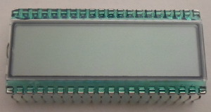
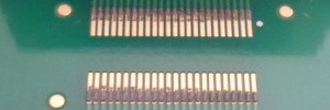
One of the annoying things is that a lot of the four-digit displays don't have the full 7 segments for all of the digits, but after looking around I found some displays that did not skimp on the number of segments. The Lumex display I selected has four full 7-segment digits, three decimal points, and a central colon (32 segments in total). It is a glass-based design that dates back from the late-1990s, so the data-sheet is a bit on the simplistic side, but it also means that does not require any fancy tricks that more recent designs might require. Although the Lumex LCD display is through-hole mounted using the standard 0.1 inch (2.54mm) pin pitch, one annoying thing is that the two rows of pins are a nominal 0.97 inches (24.64mm) apart, so it does not fit nicely onto standard breadboard.
I am not sure of the reasons why, but the normal direct current used in most electronic circuits is damaging to LCD displays, so they have to be powered using a driver that applies an alternating current across the LCD segments. The Lumex panel uses 5-volt static drive which means it uses a single back-plane (i.e. single segment common), as opposed to multiplex driving where the use of multiple back-planes reduces the total number of signal lines needed to drive the LCD display. I opted to use the NXP PCF85162 LCD driver because it is controlled using I2C and is capable of driving all 32 segments from the single chip.
Reflowing the driver chip
In the past I have written about different chip form-factors, and in particular how I preferred SOIC to SSOP due to the much wider spacing between pins, since the extra spacing made solder bridging less likely. Well the PCF85162 chip itself is TSSOP, which is even smaller than SSOP, and requires a microscope to position properly. Anyway for testing purposes I got a Proto Advantage PA0040 breakout board (Digi-key PA0040-ND; CPC PC01816), although this particular board is intended for slightly narrower chips so I took care to only put solder paste across the far ends of the pads, as otherwise there would be solder paste under the chip casing itself rather than just the pins. First time round I tried putting down a thin strip of solder paste, as shown below:
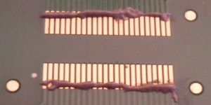
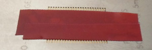
The result was basically a disaster. By the time I had cleared all the solder bridges, during which I practically drowned the chip in flux, I am pretty certain the whole thing was screwed up. I suspect some of the pins had become disconnected, there was certainly some damage to the breakout boards itself, and it is possible the chip itself was fried. It did not seem to be responding to I2C transactions, and I decided to simply write off this effort. Fortunately I managed to source a matching solder mask (CPC SD01976) for the breakout board, although I had to put some tape across the slots to make sure only the far ends of the pads got covered in solder paste:
Not an elegant solution, but the resulting solder paste application — shown below — was what I was aiming for. The solder paste did not seem to have a uniform consistency, and given my suspicions of its quality I probably should not be using it on something of this scale, if at all — if this attempt failed my intention was to open a syringe of Chip Quik (Digi-key SMDLTLFP-ND) I had yet to get round to using. Positioning of the chip on top of the solder paste was also difficult, as I wanted to avoid smearing it between pads. However once the reflow was done, the results visually looked perfect, with no short-circuits detected when I checked the breakout pins with a multi-meter.
In all of this it was not the waste of a chip that bothered me — the chip itself was only €1, but the breakout board was around €7. I have the suspicion that it would have been cheaper to get my own custom breakout boards fabricated rather than using these off-the-shelf ones.
Circuit wiring
The mapping between pins and segments on the Lumex LCD display seems to be for internal wire routing convenience, as the top and bottom segments are routed to the top and bottom pin rows respectively. The table below shows the pin mappings, alongside with which pin on thePCF85162 driver connections are to be made with. Since the right-hand digit does not have a decimal point, I used the corresponding driver signal to control the central colon, but otherwise stuck to the mapping the PCF85162 data-sheet recommended.
| Driver pin | 22 | - | - | 30 | 29 | 28 | 27 | - | 38 | 37 | 36 | 35 | 9 | 46 | 45 | 44 | 43 | 6 | 5 | 4 |
| Segment | C | - | - | 1G | 1F | 1A | 1B | - | 2G | 2F | 2A | 2B | : | 3G | 3F | 3A | 3B | 4G | 4F | 4A |
| LCD pin | 40 | 39 | 38 | 37 | 36 | 35 | 34 | 33 | 32 | 31 | 30 | 29 | 28 | 27 | 26 | 25 | 24 | 23 | 22 | 21 |
| LCD pin | 1 | 2 | 3 | 4 | 5 | 6 | 7 | 8 | 9 | 10 | 11 | 12 | 13 | 14 | 15 | 16 | 17 | 18 | 19 | 20 |
| Segment | C | - | - | - | 1E | 1D | 1C | D.1 | 2E | 2D | 2C | D.2 | 3E | 3D | 3C | D.3 | 4E | 4D | 4C | 4B |
| Driver pin | 22 | - | - | - | 31 | 32 | 26 | 33 | 39 | 40 | 34 | 41 | 47 | 48 | 42 | 1 | 7 | 8 | 2 | 3 |
The identification of segments on LCD displays seems to follow a standard pattern, as the mappings given in the data-sheets for both the display and the driver match up, and are summerised in the diagram below as letters — segment identification is approximately in clock-wise order, going round the outside first, and with the decimal point coming last. The diagram also includes the segment-pin mapping, identified as S0 to S31, based on recommendations in the driver data-sheet.
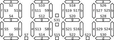
Note that mapping between segments and bit-values is big endian, so that segment c is 0x80 whereas the decimal point is 0x01. This caught me out as I assumed S0/S8/S16/S24 would be the least-significant bits, and had originally constructed my test byte-values accordingly. All other wiring was as indicated in Figure 4 (Page 11) of the data-sheet, with the addition of VLCD being wired to Vdd — in other words pins 15-20 tied to ground, pins 14 & 21 to the Vcc power rail, and pins 10 & 11 to the I2C master SDA & SDL terminal respectively.
Driver commands
ThePCF85162 driver is a write-only I2C device so it will not respond to read requests. It uses one of two I2C addresses, based on whether the SA0 pin is tied high or low, which is illustrated in the table below:
| I2C address | R/W | ||||||
| 0 | 1 | 1 | 1 | 0 | 0 | SA0 | 0 |
0x70 or 0x72 |
|||||||
The payload written to the driver consists of one or more command bytes, followed by zero or more data bytes. The MSB bit of each command byte is a continuation but, which if set indicates a further command byte is to be expected; if cleared any further bytes are display data bytes. There are five different command bytes, which are described below assuming that static drive is the desired operating mode.
Mode set
By default the driver has the display switched off and is in 1:4 multiplex mode, so0x49 can be used to get it into the correct operating configuration. The display bit can be used to manually blink the display, although such effects are better done using the built-in blink mode. Bias is not used in static drive mode.
| Cont. | Opcode | Unused | Display | Bias | Drive mode | ||
| C | 1 | 0 | 0 | 1 | 0 | 0 | 1 |
| C | 0x49 (0x41 for display off) |
||||||
Load data-pointer
The data-pointer gives the bit-address within the LCD RAM that data is written to, although things gets a little fancy in the multiplex modes. In static drive mode the data-pointer is incremented by 8 each data byte, and using0x00 resets the data-pointer to zero. I had assumed this 8 was bits, but inputting 4 bytes did not produce either the overflow nor the wraparound I was expecting based on the data-sheet.
| Cont. | Opcode | Address | |||||
| C | 0 | 0 | 0 | 0 | 0 | 0 | 0 |
| C | 0x00 |
||||||
Device select
ThePCF85162 uses a system where multiple drivers can use the same I2C address, but respond differently to data payloads based on a second subaddress, which is supposedly incremented when the data-pointer overflows. For a single driver with all the subaddress pins tied to ground, this is implicit behaviour that is not wanted, so 0x60 would reset the subaddress counter and avoids suppression of display data loading. In practice I have not seen the need for this command in the single-driver single-display static drive setup presented in this article, as the expected overflow does not seem to be triggered.
| Cont | Opcode | Subaddress | |||||
| C | 1 | 1 | 0 | 0 | A0 | A1 | A2 |
| C | 0x60 |
||||||
Blink select
In static drive and 1:2 multiplex modes, there are two ways the display can be blinked: On-off (Type=0), and switching between the two LCD RAM banks (Mode=1).
| Cont | Opcode | Type | Frequency | ||||
| C | 1 | 1 | 1 | 0 | 0 | 0 | 0 |
| C | 0x70 |
||||||
Clearing the Type bit results in on-off blinking, whereas setting it results in alternating between the two LCD RAM banks in the drive modes that support having two banks. The blink frequency depends on the driver clock frequency, but using the internal clock and assuming its typical frequency of 1.85kHz (specified range is 1.44-2.64kHz), results in the blink frequencies listed below:
| Operand | Frequency division | Effecive frequency |
| 0 0 | n/a | No blink |
| 0 1 | 768 | 2.4Hz |
| 1 0 | 1536 | 1.2Hz |
| 1 1 | 3072 | 0.6Hz |
Bank select
In static drive and 1:2 multiplex two banks of RAM are available, and the ones used for both data-input and data-display can be independently selected. However for most use-cases setting both to use Bank 0 (the default) using0x78 is the easiest thing to do. Although the data-sheet mentions page-flipping, the only practical use of having two buffers I can think of is using blink select to have a flashing colon or decimal point.
| Cont | Opcode | Input | Display | ||||
| C | 1 | 1 | 1 | 1 | 0 | 0 | 0 |
| C | 0x78 |
||||||
Testing
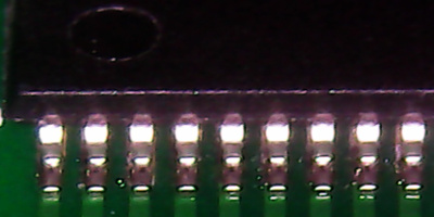
Since the connection between the LCD driver and the LCD panel is effectively a parallel interface, the wiring gets a little messy, as can be seen in the picture below. The driver groups the segments for each digit together whereas the LCD panel splits them between the two sides, so there are a lot of crossing wires, which would also make designing an equivalent PCB quite tricky.
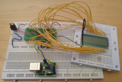
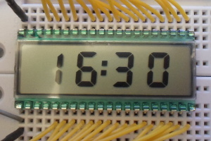
To test the LCD panel & driver I used the USB-ISS I2C master together with my ttyTxRx.py Python serial script. Immediately after a power-up reset the following command-line is the bare minimum needed to display 16:30 on the LCD panel:
./ttyTxRx.py /dev/ttyACM0 1 54 70 5 49 c0 be ea f7
Using the following command will cause the colon in the middle to start blinking. It works by setting the driver to alternate between the two display banks, and the content then loaded into this second bank (0xc0beeaf6) is the time value with the colon bit cleared.
./ttyTxRx.py /dev/ttyACM0 1 54 70 7 fa f6 00 c0 be ea f6
Pay attention to the continuation bits — they are all too easy to accidentally set or leave cleared, which usually makes the driver unresponsive. Segment S9 of the second digit (segment b, second left) was non-responsive, which I tracked this down to a poor connection between driver pin 35 and the break-out board, but all other segments were operational. I decided against reworking the chip, at least for the purposes of this article, on the basis there was a good chance I would damage the chip rather than fix the disconnection.
Power consumption
Measuring the current flowing out of the voltage regulator gave a reading of 0.02-0.03mA, which corresponds with the 3.5μA the data-sheet states should be expected from a 5-volt circuit. Whether the LCD display was connected — and if so how many segments were lit — made no noticeable difference to the current draw, which was right at the edge of what the multi-meter was able to measure. For comparison, the PIC16F88 LED timer was 3.7mA per segment — LCD displays work by blocking light rather than emitting it, which is why actual power consumption is so low that even minimal amounts of static is enough to turn “on” LCD segments.Remarks
My original intention was not to try out LCD displays until I had finished all my LED display projects, but delays in getting the PCBs for the latter meant I ended up trying out LCD displays & drivers early. The TSSOP-sized driver chip was a challenge, but with a solder mask the reflow went smoothly, with the one disconnection probably due to the poor quality of the solder paste I used. In the longer-term I reasonably expect to make such a daughter-board PCB for this driver & display, although I expect the amount of crossing-over wires to make it something of an ordeal.The experience on getting the LCD driver & display pair working was a mixed experience. Getting the TSSOP driver chip reflowed to the breakout board was quite an ordeal, with the first attempt being bricked and the second attempt still having a disconnected pin, but once that was done things mostly just worked. I got the display data endianness wrong, but otherwise the smoke-test I2C command sequence I wrote based on just looking at the data-sheet worked first time. Some of the finer details regarding sub-addresses and the data pointer do not seem to behave as the data-sheet suggests, but they are not really a concern in the use-case presented here.
To tell the truth the vast bulk of this article was written before I actually wired up the test circuit, and I was surprised at how little needed to be changed once the hardware setup was complete. The next logical step is to create a PCB that makes this hardware a self-contained I2C module, but for now such a module does not satisfy a project need that is not already covered using alternative components. Nevertheless the cost of getting the LCD components over from the US means that this will change.