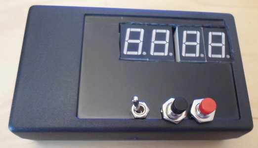
PIC16F88 Timer PCB
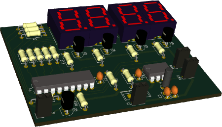
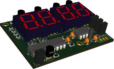
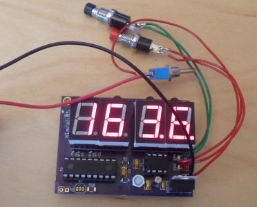
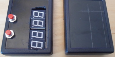
19 March 2018This circuit is a PCB version of the PIC16F88 LED timer which has been designed & built to be installed into a small project box, with the end goal of feeling like a finished product. For PCB design this is my second time opting to use KiCad, in addition to being an opportunity to try out an alternative PCB fabrication service. The circuit itself is functionally almost identical to that built on prototype breadboard, so this article will not cover electrical details. Although I did provision for an audible alarm, space constraints meant that I did not include one in the end. I built two units, with mistakes in the first being taken account of when constructing the second, the completed latter of which is shown below.
The circuit itself is functionally almost identical to that built on prototype breadboard, so this article will not cover particulars of the electronic components. The main investigatory goal of this project is in mechanical details such as PCB anchoring and preparation of the project box, which includes ordering in of both parts and new tools. Measurement accuracy would be a major concern, as tolerances have not previously been a significant issue.
Circuit design
Although I did some circuit layout in Fritzing when making the prototype board, a significant portion of that circuit was built ad-hoc. The PCB schematic laid out in KiCad was basically a reverse-engineering of the prototype, and being much more complex than the TCA9535 breakout PCB meant it was also a more complete experience of using KiCad. The schematic is shown below, although typical of eeschema screen-shots it is ugly even before it is scaled. Nevertheless all the components & connections can be worked out, and it follows the outline schematic of the prototype.
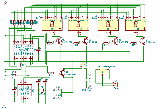
Aside from adding in a transistor-controlled port to power an alarm, the circuit is the same as the prototype I built on breadboard, so I could re-use the same firmwares I developed previously. The schematic component for the 7-segment LED display bears no resemblance to what the actual component looks like, which is quite irritating in cases like this where there are multiple combinations of correct pin wirings — the important factor in deciding pairings of microcontoller and LED display pins is convenience in routing, and with the breadboard prototype I chose pairings that would avoid wires crossing over each other. Had I not already worked out pairings, getting this right would have been a major headache, and I most likley would have made my own schematic component rather than using a stock one.
Power supply options
I looked at multiple options for circuit power supply, including having ordered in several different forms of battery holders as well as some USB sockets. However when wired up to the prototype board, two 3-volt button batteries (using Farnell 3029827) had a tendency to cut out, and 5.1V (measured) from USB did not work at all. I traced this to theLM7805CT (Farnell 1696994) power regulator having a minimum input voltage of 10V, although in practice it works fine when powered by a 9-volt square battery. For 5-volt output there were some voltage regulators that had a nominal minimum input of 6 volts, but I suspected that a margin would be needed to account for partly-discharged batteries. That basically eliminated all the circa 6-volt battery holders I bought in.
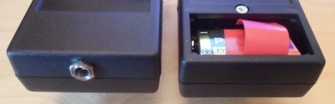
In the end I concluded there were two viable options for the power supply: External DC power using a 2.5mm power jack (Farnell 2285054), and internal power using a 9-volt square power cell (a stock of connectors from Maplin just before it went bust). Which one to use was down to space constraints, and in the end both ended up getting used — the DC connector on the first box, and 9-volt power cell on the second. These are shown in the picture below on the left and right respectively.
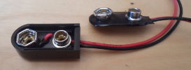
Originally the first unit was supposed to be powered by a 9-volt cell as well, but when connected to the power lead it would not fit into the power cell bay, so I simply cut off the power lead head and soldered in a DC connector instead. By this point I had realised that I had forgotten to add in a power switch, and with an accumulation of bodges decided get something working before I comletely damaged what I had. For the second unit I used a thinner power lead that did fit when connected to a power cell. Both of the power leads are shown below for comparison.
I had originally opted for the thicker plastic connectors, because I have memories of how the thinner ones soon break apart even with careful handling. The thinner ones were still a bit of a pain, but at least it was possible to get the attached power cell in and out of the power bay.
PCB real-estate budget
My original plan was to use just through-hole connections, in part so that the selection of components used on the PCB would be the same as used on the prototype breadboard circuit, and in part because I wanted a break from reflow soldering. As can be seen in the 3D model of the resulting PCB design shown below, the location of most components is is pretty much the same as the prototype, with the PCB's dimensions being 75mm by 60mm. For some reason there is no 3D model for the voltage regulator, so it is not shown — it would be located just behind the recepticle in the middle-front, where its PCB outline can be seen.
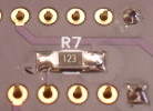
The PCB size of 75x60mm turned out to be problematic when looking for a suitable project box — all the ones I found that were big enough felt too big, and tended to be somewhat expensive for what they were. I suspected that moving components around would not reduce the PCB size much, so in the end I decided to change the resistors to surface-mount components, and I targeted a PCB size target of 60x45mm, which would have allowed it to fit even the smallest project box I had stocked. The 3D model of this redesigned board is shown below. Although it cannot be seen, the pull-up resistor for the MCLR pin on the larger micro-controller is on the underside of the PCB, and it uses a footprint with extra-large SMD pads to aid hand soldering. I intentionally used different physical sizes of resistors for the two different resistor values
The ability to show a 3D model of the PCB is a very nice feature of KiCad, as it gives a better sense of how close components are than a 2D PCB view, and for this board it felt that things were quite tightly packed in. My biggest concern was the amount of space around the screw holes, although in the end they seemed to be just about big enough. The big down-side of the 3D view is that it does not account for the fact that the LED chips would actually be mounted on top of receptacles, and the absence of a voltage regulator 3D model meant that I almost forgot how tall it was.
PCB Fabrication
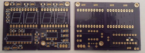
In the past I have always used Aisler for PCB fabrication purely because it is the foundry that Fritzing points people towards, and although reportedly somewhat pricey, the service was nevertheless good for my needs. This time round I decided to look at alternative fabrication services, in part to see how they compared. Since all the Chinese ones had shut down for the lunar new-year holiday, I opted for the US-based OSH Park — they quoted $21.40 for three PCBs with a two-week turnaround time, although I got lucky and my PCB was used as filler on a board that was part of the 5-day express service.
Even though it was sent via post and did not need a signature, the delivery was tracked with a granularity normally expected of a courier. Shipping took 19 days which was longer than expected, but to be fair 8 of those days were between it arriving in Europe and it landing in my mailbox, notionally due to the bad weather at the time. For reasons unclear to me, the shipment included a packet of Welch's Fruit Snacks, which is an odd thing to pack together with electronic circuit boards.

Soldering & assembling the PCB
The fabrication service I used does not provide a solder stencil cutting service, but since the resistors are spread out rather than having their pads close together, I expected that this would not be a major issue. Two PCBs were assembled, one using hot-plate reflowing with solder paste manually laid using cocktail sticks, and one where I hand soldered all the surface-mount components using my soldering station. The first is shown in the image below.
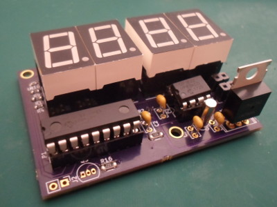
My stock of solder paste is likely well past its shelf life and was probably of dubious quality to start with, which would explain why it was such a pain to place it onto the component footprint pads, but after the reflow all the surface-mount components seems to have come out well. There was one surface-mount component on the under-side of the PCB that I gave an extra-large landing pad to aid hand-soldering, shown in the picture below, and as it turned out soldering it was problem-free — the ease of soldering this latter resistor is why I decided to try hand-soldering all the surface-mount components for the second PCB. The resulting solder joints did not look quite as nice as those on the reflowed PCB, but it was a lot easier & quicker than manually laying the solder paste.
For the NPN transistors I used the TO_SOT_Packages_THT:TO-92_Inline_Narrow_Oval PCB footprint, which assumed transistors with straight legs, whereas the BC547BTF (Farnell 2453790) transistors I used have legs that are bent so they fan out. As a result I had to straighten the legs out using a pair of pliers, as shown in the picture below — instead I should have TO-92_Inline_Wide footprint to avoid this little headache.
![]()
Trying to place the 10-way pin receptacles for the LED chip pairs was a noticeably tight fit, which I initially put down to the footprints being slightly too close to each other, but in hindsight suspect may be an issue with the LED footprints themselves. On the plus side, it made a nice change not having to worry about them falling out of place during soldering. The clearance of the voltage regulator was higher than the LED chips, so I had to bend the top part to a right-angle in order to reduce the clearance. This was planned, but is definitely not elegant — In hindsight I should have looked into regulators with a lower profile, such as the TI UA78M05IDCYR (Farnell 2781825) but there is no guarantee it would have fitted in the space available.
Wiring things up
I left off the alarm transistor & connector as there was no room within the case for the sounder. One of the mistakes I made with the first unit was to use solid core wire, as it is relatively hard to flex, which meant putting everything into the case was difficult. In particular there was the tendency for the wires to pop out of the receptacles, and desoldering the one used for the power connection turned into quite an ordeal. For the second unit I decided to use multi-stranded wire that is easier to flex, which also required direct soldering onto the PCB.
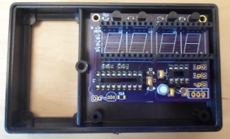
Since the bottom screw hole does not correspond to a mounting hole in the box, I bolted in a nylon spacer to keep the board flat. The nut does come a bit closer to components than I am really comfortable with, but there is sufficient clearance that there is no short-circuits.
Mounting in box
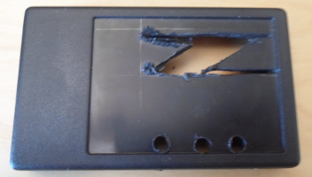
My original intention as a first iteration was to use a 74x50x28mm project box I sourced off E-Bay, as this size felt a nice size in relation to the size of the LED display. They were also relatively cheap £1.55 each (shipping was free) so I was not too worried about making a mess of the box, which as shown below is what I did. However after some drilling & cutting it became apparent that it was that bit too small, with insufficient clearance between the PCB components and the buttons.
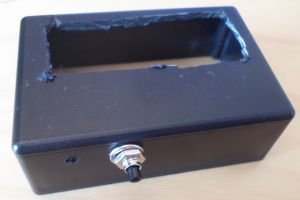
After giving up on the above project box, I used an alternative box I also found on E-Bay that included a separate power source compartment. The external dimensions were 104x64x28mm but at the time I ordered it the E-Bay listing did not include a schematic, so I had the headache of manually working out the dimensions — as it turned out the most critical measurement of the mounting hole separation was a nominal 55.55mm but by own measurement of 55.50mm was close enough that the difference did not matter, with the PCB matching up without apparent problems. Including delivery it was somewhat steep £4.53, but most good project boxes seem to be around this price.
LED display slot
Cutting the slot for the LED chips was trial-and-error, as for the first unit I did not have any real points of reference to draw out cut lines, although in hindsight the only real mistake was cutting too far to the right. Unfortunately the right edge of the right-most LED chip was beyond the recessed area, which as well as looking unsightly, was also a problem to cut. However, even though this first attempt was something of a mess, I was able to use it to draw approximate cut lines on the second attempt box.
Initial cutting was done using a rotary tool (Dremel 300 equipped with a cutting disc), and after this somewhat messy rough cut that is shown in the picture below, I used a nibbler to cut away the pieces that were preventing the LED display from slotting into place. I used much the same method first time round but made a much better job of it for the second unit. The one big difference in method was using a file to cut the right-hand side, since the raised area was too thick to fully fit into the nibbler.
Fitting in buttons
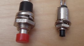
For such a simple device choosing a button to use was more complex than I expected, and for this project the choice was of two sizes I had in stock, which are shown in the image below. From a purely aesthetics perspective I tended to prefer the larger button (red one in picture), but what ultimately ruled out the smaller size was that the length of the neck was not enough to reach through the thickness of the casing. The source of the buttons was a combination of E-Bay and Maplin, which is less than ideal as E-Bay is not exactly the best of places for guaranteed re-orders, and Maplin has now gone bust.
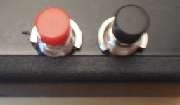
In both units I drilled the holes for the buttons that bit too close to the bottom edge of the recess, and as a result the retaining nut overlapped with the raised edge towards the edge of the box, which is both unsightly and results in a less-than-secure positioning as the tightened nut doe snot have much to rest upon. To keep the nuts flat I cut a segment out of the washers so that they would fit around the buttons, and this is shown in the picture below.
Doing this cutting is probably within the “do not do this in the home” category of endeavours, which I blatantly did do within my own flat. I needed to take a bit of care where the sparks were flying, and unlike most people I keep both a powder and CO2 fire extinguishers in my flat.
Conclusions
The ultimate aim of this project was to create a timer that was an object rather than an exposed circuit, and on this criteria it has been a success. As a multi-stage project this is comparable to the LED matrix display, and has been in the making for a similar amount of time, albeit somewhat more on-and-off. A comparable number of issues came up, although this time round they were spread over more than one article. Below is the main areas of reflection that spring to mind.KiCad experience
The single biggest thing I did not really take on board until after I had laid out the schematic in Eeschema is that there is no need to exhaustively draw out all the wire connections. Instead all wires that have labels with the same text attached are all implicitly connected, as are all power supply symbols such asGND and +5V. I probably should have also looked at buses rather than running a load of parallel tracks for the high-side LED display power, but there was limits to how much new stuff I wanted to try out first time round, and for revision two I felt it better not to completely redo a known-correct schematic. Other bits of information that would have been useful to know before I started are detailed below:-
- Placing track Vias
- Vias need to be placed while drawing a track, which takes some getting used to. The
Vkey toggles between the front and back copper layers, and a via is automatically placed if the last segment of track is on the opposite side. Unlike with Fritzing, there does not seem to be any way to add a via to an existing track. - Using the
PWR_FLAG - The
PWR_FLAGsymbol indicates where a power supply will be attached to the circuit, and leaving it out is the cause of the “component X is not driven” electrical check warnings. The other power symbols are actually special cases of wire labels, rather than indications where the circuit will be powered. - Display modes have different editing support
- KiCad pcbnew has multiple rendering modes, Default, OpenGL, and Glade — and they are more than just different drawing back-ends. The way they operate is also different, most notably with how tracks can be drawn & edited, with OpenGL/Glade having more point-and-click support.
- Hiding redundant markings
- Within the Visibles panel on the right-hand side, turn off
F.Fab&B.Fabunder the Layers tab, andValuesunder the Render tab. These correspond to things that do not appear on the final PCB, so I prefer not having to deal with them.
Soldering
I am thinking of reflowing the third PCB using my stock of alternative solder paste just to see how it compares to my usual solder paste, but after this project I am now more inclined to hand-solder rather than reflow solder in cases where I do not have a solder mask. Molton solder handles a lot better than solder paste, and even for SMD footprints that are not intended for hand soldering it is surprisingly quick and easy. I wouldn't hand solder a SSOP/TSSOP chip, and am unsure about even hand soldering much larger SOIC chips, but hand soldering has the added advantage of being substantially less messy than handling solder paste. It can also be started and stopped at will, whereas for a reflow at least 30 minutes has to be set aside, and in practice could end up taking an hour including setup & cleaning up.Box cutting
The process of milling project boxes is easier said than done, and I tried out many different ways of cutting: Coping saws, drills, rotary tools, nibblers, tape reamers, and files. As well as the cutting tools, there is also passive tools such as clamps to hold things in place. All in, some things worked well, some things could have been better, and some things were an outright waste of money. Being completely new to the problem space, this was to be expected, and in hindsight the following details what I think are the tools to have in very approximate order of importance:- Tape reamer
- This is a tool I remember seeing when I was doing electronics at school, but could not remember its name. A variable diameter boring tool, used for cutting a precision diameter hole for components, in particular switches and connectors. You will need one of these.
- Nibbler
- Really intended to cut sheet steel, it works by taking a square “nibble”, which allows an opening to be cut incrementally. An initial starting point needs to be cut or drilled using an alternative tool, but once that has been done skilled use of a nibbler can cut away a lot of material surprisingly quickly. A lot easier to control than a saw.
- Drill
- Nibblers and reamers need starting points, and a drilled hole is the simplest starting point. At best going without a drill will make things a lot harder than they need to be. I used a cheap (circa £15) one off E-Bay, which is good enough for pilot holes, but I would not use it for precision drilling.
- Vice
- Things gets hard if you are trying to cut material from something not held securely. I happened to come across the Maplin vacuum base vice, which is brilliant for people like me who don't want or have a permanent workshop bench, and unlike a vice from a hardware store is designed to grip plastics and circuit boards rather than wood.
- File
- Filing takes away less material than other forms of cutting, so the final edge is made with much more precision than is possible with other tools. A lot of work though, so will only want to use it for finishing.
- Rotary tool
- Rotary tools are something that I don't remember seeing when I was younger, but they are basically a variable-speed drill intended for cutting & polishing rather than making round holes. They are marketed as multi-purpose but I personally think they are specialist tools unsuitable for drilling. Cuts quickly, but can easily leave a mess as it tends to melt plastic.
I'm not much into 'elf & safety culture, but safety glasses is one thing not to skip, especially when using the cheaper tools that are more likely to come loose and/or break — some of the tool bits I have seen don't seem to have much holding them together, only a small bolt that is probably not designed for the stresses involved. Particularly if you wear spectacles, the square transparent safety glasses that are commonly used in chemistry classes are preferable, as they have much better ventilation.
Boxing things up
In hindsight I should have put the LED chips about a millimetre further to the left on the PCB so that I did not need to cut into the edge ridge of the project box, although to make room I probably would have had to put some of the resistors underneath the left-most LED chip. Had I made the board use all four mounting holes in the project box, something that I originally intended to do with a second-revision PCB, it is possible that there would not have been enough clearance for the buttons. However given the available information at the time, which included the possibility that the mounting holes may be in the wrong positions, I felt that the PCB itself was a reasonable balance of compromises.I think trying to use a project box without mounting holes was asking for trouble, particularly for a circuit that has external components that are attached directly rather than via wires. Had the schematics been available earlier I would have laid things out much better in advance, although there is no guarantees that I would not have run into other problems. I feel that the size of PCB the project box is designed to hold is actually a good size, although I suspect the battery compartment would have to be used for other purposes as there is not much clearance above the PCB area itself.