LED matrix display, 2nd gen.
15 July 2018When I started doing electronics projects my early focus was on dot-matrix LED displays, initially manually wired then I came across the Multicomp
703-0193 LED chips (Farnell 2112219), which culminated in my LED matrix display. Recently I decided to look again at displays using the same LED chips, thinking of making a tile module much like the LCD time display, and this circuit project is the result.
Main personal point with this project is realising how far my electronics ability had come since the previous version of this project. Last time round the row driver occupied one of these 10cm strip-boards, whereas this time the whole circuit is on one of them. Getting in-circuit flashing working helps makes this a mile-stone circuit for myself.
Design choices
The original LED matrix display was built up gradually from separate circuit boards, most of which were PCBs, whereas this circuit is intended to be self-contained. I2C will be used for external communication, a role done using RS232 by the previous LED matrix control system, the longer-term idea being that this new circuit is a potential prototype for a tile intended for a larger display. An outline schema is shown below:
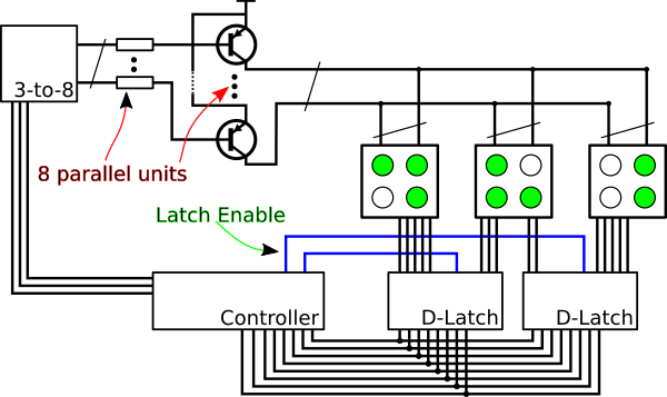
The main idea is that, rather than all the LED chips being part of the same refresh cycle, different areas of the LED display handle refreshing autonomously. In particular this gets around the biggest problem with the previous circuit, namely that the row driver had to source a lot of current.
Main controller
In the past thePIC16F88 has been my usual choice of chip for anything not needing I2C master capability, due to having a decent selection of features and being a nice size of 18 pins (i.e. two full 8-bit ports), but for this circuit I opted for the PIC16F1828 instead. The F88 is relatively expensive — about 50% more than the F1828 individually — and in any case I had been thinking about consolidating on the PIC12F18xx/PIC16F182x sub-set of PIC microcontrollers. The F1828 is the chip with the largest number of I/O pins within this family.
In-circuit programming
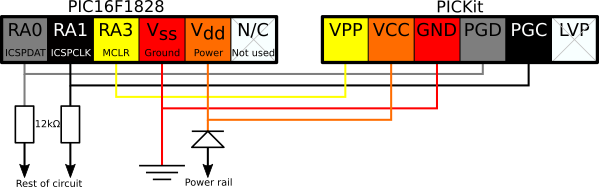
Moving a microcontroller between a programming seat and a socket on the circuit board is a choir at best, but the previous attempt at integrating a programming header into a circuit ran into problems — problems that were only solved after I had finished building this circuit. For many of my circuits since then provisioning programming headers has been impractical, but not having successfully included in-circuit flashing on any circuit since my original LCD display felt like unfinished business, so for this circuit decided to have a serious attempt at getting it working. I could have dedicated pins to chip flashing but I felt that was a cop-out as I/O pins are a valuable commodity, and the alternatives are not consecutive bits on the same port. The schematic below summarises the isolation measures tried this time round: Pins that are dual-purposed with chip programming should not be driven or loaded, which means not attaching pull-up/pull-down resistor or capacitors, and many sources I read recommended isolating the rest of the circuit with 10k+Ω series resistors. In this circuit they are attached to the address pins of the74AHCT138 so the low current in normal operation is not an issue. The diode did not isolate the rest of the circuit as I expected, but in any case flashing the microcontroller when the circuit was running under its own power proved to not be an issue.
After I had finished building this circuit and successfully connected to it from the chip programmer, but before I had started writing the firmware, I went back to the RS232 LED display that was the last time I seriously tried including in-circuit flashing and quite quickly got it working. Between the two circuits — which I got working the same weekend — I concluded that in-circuit flashing is more robust than I thought it was, and my previous aversion to using it was unjustified. This has greatly increased my confidence in relying on it, which is important as I had been planning on using surface-mount microcontrollers which cannot be easily programmed out-of-circuit.
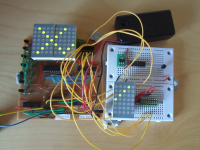
LED matrix modules
For simplicity I decided to re-use the matrix modules from last year's LED matrix display, which is a breakout board that mounts an703-0193 LED chip, with each column sink pin having a 390Ω current-limiting resistor. These modules have a much more convenient pin out than the overlying LED chip, take up less real-estate on the circuit board, and all-round were cost-effective to re-use. 6-way header receptacles are a lot cheaper than 7-way ones, and the pins on the matrix modules are also a lot more robust.
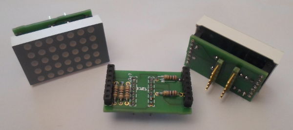
In hindsight there are two things I did not get quite right with these modules: The pinning and the protective resistance. With the pinning I used left-to-right, as shown in the receptacle-view table below, which resulted in a discontinuity with the pin for the 7th row. In hindsight putting Row 7 at the other end of the bottom row would have been a better choice, but back in the latter half of August 2017 when these boards were designed & ordered I was still figuring stuff out. This is a minor complication with the refresh cycle within the firmware.
| Row 1 | Row 2 | Row 3 | Row 4 | Row 5 | Row 6 |
| Row 7 | Col 1 | Col 2 | Col 3 | Col 4 | Col 5 |
The other issue is the choice of 390Ω protective resistors, as I suspect the resulting expected current draw is pushing hard against the DC specifications of the LED chips. Assuming a voltage drop of 2.6v across the protective resistor, which in a 5v circuit allows for the “typical” 2.1v across the LED chip and 0.3v for the transistors & latches —, the expected current draw is 6.7mA. In this circuit each individual row has an effective 1:7 duty-cycle, but assuming the switch-over time is negligible there is always one row active, so the worst-case of all dots lit is limited by the continuous-current limit of the LED chips rather than the peak-impulse limit — this works out at 6mA per dot (i.e. per column since rows are cycled), which is less than the expected current draw. For simplicity I decided not to add extra resistance in series within the circuit itself, although this is something that will be done later to investigate the effect of increased protective resistance on LED chip brightness. The accuracy of the power-related assumptions will also be considered in a later section on circuit measurements.
LED current source
I originally planned to use an74HC238 3-to-8 decoder to source the current for the LED rows, primarily in order to reduce the number of pins required by the main controller, but the 25mA that each output pin could provide was way below requirement. With all dots lit a row would draw 100mA, which meant that instead individual BC556 PNP transistors would supply the power. Since PNP are switched on by active-low, I exchanged the 74HC238 for a SN74AHCT138N which has its outputs inverted, so the active output is low with all other pins high. I think the only difference between 74HC138 & 74AHC138 is current rating, so either could have been used — see later discussion on chip variants.
LED current sink
Before starting I had decided that I did not want large current flowing through the main controller, and initially thought about doing the actual current sinking with aSN74AHC05 Hex Inverter since it had open-drain outputs, but eventually settled on using SN74HCT573N D-Type latches to act as the current sinks. Almost as a side-effect this allowed three LED modules to be wired up by multiplexing the single RCx controller port, which had logistical advantages as well as allowing three LED matrix modules to be controller rather than two. I last used the SN74HCT573N as part of my first PCB, but after finding that parallel interfaces were a pain to deal with went looking for parallel-serial converters, and eventually stumbled across I2C I/O Expanders which since became a staple item of my circuit projects. Aside from using up stocks of chips I had lying around for almost a whole year, it made a nice change using something other than the magic bullet of I2C for internal circuit communications.
Building the circuit
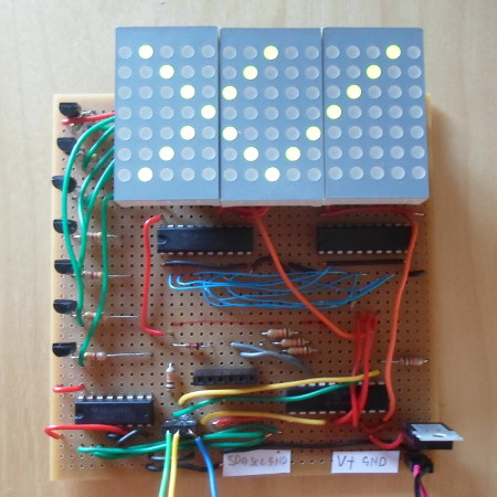
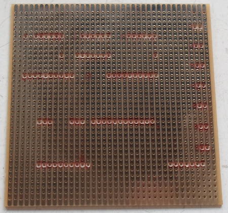
For this circuit I opted to use some of theE01238x38 strip-board (Farnell 2503759) that had been gathering dust, which turned out to be a good move since a lot of connections between chips were made by placing the pins on the same track. In fact the only chip that needed a lot of wires was the main controller. Because tracks need to be cut, using strip-board required more up-front planning than the matrix board I used in the previous project, but flip side of the coin planning out a circuit is a lot easier with strip-board than it is with various perf-boards. Below is the strip-board between track cutting and the first soldering — although I did need to cut another 2 or 3 track holes after assembly started:
After the problems with wire in a previous circuit I decided to try some AWG30 wire, which on the whole was a bad decision. While nicely flexible, stripping it is a delicate process in which it is very easy to instead break the wire, and because of the small diameter the sheath does not stop the unexposed part of the wire slipping through the prototype board holes. The fundamental mistake was that I selected wire that was half the diameter of AWG23, whereas I should have gone for half the cross-sectional area (i.e. about AWG25).
Chip variants
Aside from the Microchip PIC processor, all the chips used in this circuit are multi-source ones where the central part of the manufacturer code gives the generic part number, and the prefix/postfix are manufacturer-specific identifiers — in the postfix case related to form-factor. For instance theSN74AHCT138N is the Texas Instruments variant of the 74AHCT138 that comes in through-hole form. I previously did not pay much attention to this, but there are quite big variants in price & availability of different form-factors. From a bit of digging, the central part of the code are for chips that are part of the 7400 series.
Chip receptacles
With the exception of my first PCB and two projects where I made use of the relatively largeMCP23017 I/O expander chip, I have always made use of chip sockets rather than soldering integrated circuits directly to a circuit board. For this circuit I decided not to bother with chip receptacles and simply solder all of the chips directly onto the strip-board, on the basis that I was unlikely ever going to remove them, and if the worst happened then I had confidence in my ability to remove components. The notable thing in this case is that I soldered a microcontroller directly, whereas in the past all the chips I soldered were ones that did not require flash programming — this time round I decided to push boundaries with my luck, and save the cost of receptacles, and it paid off.
LED matrix availability
Farnell regards the Multicomp LED matrix chips as a legacy product which they are only going to stock until the current supplies are exhausted — to my knowledge I bought the last of703-0195 (column-ground red units) but the others at time of writing have the following stock remaining. My gut feeling is that these stock levels will mean that orders will be limited to people such as hobbyists who are happy with a once-it's-gone-its-gone supply, but for such people the remaining stock ought to last a year or so easily.
| Multicomp code | Colour | Polarity | Farnell code | Farnell stock |
703-0192 |
Green | Row cathode | 2112217 | 219 |
703-0193 |
Green | Column cathode | 2112219 | 632 |
703-0194 |
Red | Row cathode | 2112221 | 224 |
703-0195 |
Red | Column cathode | - | Gone |
There are Kingbright units that I think could be drop-in replacements judging by the data-sheets — they seem to be mechanically (i.e. form-factor & pin-out) identical and have similar electrical values — but they are significantly more expensive particularly when not bought in bulk. For instance the 703-0193 (green dots and column pins are ground) are €1.58 each, but the corresponding TC12-11CGKWA (green) are €3.83 (€2.57 for 10+ units).
The firmware
The firmware for the circuit — which at some point I expect to put into Bitbucket with implementation-specific comments — does not bring up many issues I have not already discussed in the past. The design is a loop that cycles through the rows and lights the appropriate columns, with a duty-cycle waiting loop that handles incoming updates. Nevertheless below are a few general points that I feel a few words here are appropriate.Latch timing
For a D-type latch to store the input value, the input needs to be stable for at least the setup time before the latch enable goes low, and has to remain stable for at least the hold time afterwards — for theSN74HCT573N these are 12-13nS and 5nS respectively. In contrast the minimum instruction cycle time the PIC16F1828 supports is 200nS (see Table 30-1 of data-sheet). Since there is an instruction for the setting & clearing of individual bits, I felt the toggling code is best written entirly in assembly:
BSF _PORTB,5 NOP BCF _PORTB,5 NOP
In theory it ought not be possible for firmware to pulse the latch enable lines too quickly, but the NOP at least negates any issues of when during an instruction cycle that output pins get modified.
Clock stretching
An issue with using I2C is the time between the MSSP hardware receiving & acking subsequent frames, which in the past a treated as an instruction budget issue linked to the microcontroller base clock frequency, whereas for this circuit I2C clock stretching is used to prevent a reception overflow by holding back the master from the next transmission. All I can really say is that had I known how easy it was to do, I would have used it previously.Timer accuracy
The specification of timers within the PIC chip data-sheets is a long-running bug-bear of mine. The data-sheet claim that FOsc/4 (i.e. the instruction-rate — a quarter of the base clock frequency) is used as timer input, but indications are that in reality the input is actually the full FOsc. Following the data-sheet the Timer2 parameters should give a delay of ~8.2mS which is clearly unrealistic given the total 18mS refresh time, but using FOsc results in a notional ~2mS delay which is within bounds of explainable error.Row ordering
As a result of the pin ordering of the LED matrix modules, the order of the rows on the LED chip does not match the address order of the74HC138 current source. Therefore what would ideally be some simple bit-masking has to be replaced by an if-then-else chains, so that ordering within the internal buffers are representative of the order on the physical LED display. My personal view is that this mapping is best kept in firmware, otherwise the firmware would need a mechanism to provide external software with ordering information, which I concluded would be a bigger headache.
Brightness tests
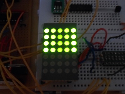
One potential issue with the LED matrix modules is the aggregate current draw, but if the on-board protecting resistance of 390Ω is to be increased, this has to be balanced against reduced brightness. As a result some brightness tests were done with extra resistors hot-wired in series with the current sink pins of one of the LED modules — as shown below — to see how the resulting brightness compares.
In all cases the difference compared to the built-in 390Ω brightness was noticeable, and in day-light conditions I thought that 680Ω was just about alright; in darker conditions the differences were less noticeable between the higher resistance values, but other things being equal I would not opt for them. Pictures showing LED brightness do not really do any justice, but in the one below four different values were tried: The far-left and far-right columns used the base 390Ω on the LED modules, whereas the three middle columns, going from left to right are 655Ω, 1050Ω and 680Ω respectively. 1,390Ω was tested separately but this was far too dim for my liking, as was 480Ω for which I could not see any difference compared to 30Ω.
From a brightness perspective I would be reluctant to increase the protective resistance more than about 100Ω, so if it was to rebuild the modules — or use the LED chips directly — I would consider using at most 500Ω resistors. For a 5volt power supply and the typical 2.1v drop across the LED chip, the remaining voltage drop across such a resistor would draw 5.8-6mA, which is the limit if the total LED chip draw is to remain within 30mA with all dots lit. However the unknown is the voltage drop across the transistors used to switch the rows & columns.
Circuit measurements
Although I have in the past done circuit measurements they have typically been with static conditions, so this section is as much about validating multi-meter measurements of dynamic conditions as cross-checking data-sheet values. The measurements were made for one of the columns with a single dot lit, and these are detailed in the table below. A more useful calculated aggregate is also provided which covers all seven rows, which in most cases is obtained by simple multiplication.
| Metric | Raw | Aggregate |
| Voltage drop | 0.650-0.685V | 4.55-4.80V |
| Current draw | 0.97-1.00mA | 6.79-7.00mA |
| Frequency | 55.78Hz | 17.93mS |
| Duty cycle | 13.8% | 96.6% |
The voltage drop is across the entire LED matrix module (i.e. both the LED chip and the protective resistor) and although there is a lot of fluctuation it is around the expected 4.7 volts. The current draw is a little higher than expected, which is probably down to the voltage drop across the LED chip being a bit lower than the data-sheet specified “typical” value. Only issue here is that the expected values are already pushing the upper end of the LED chip specifications, and since an extra 100Ω did not seem to affect brightness, I will in future opt for 500Ω over 390Ω protective resistance. A frequency of 55.77-55.79Hz corresponds to a period of just under 18mS, which is believable as I adjusted timings until even with close inspection I could not see any flicker on the LED chips, and when I considered the refresh cycle of the previous LED matrix display I concluded that 25mS (about 40Hz) was when flicker became noticeable. In addition, an aggregate duty cycle of 96.6% is in line with my expectation of there being a row lit all but a negligible proportion of time. Only issue is that it calls into question timer accuracy, as the calculated ~8mS delay is clearly impossible.
The last words
Architecturally this circuit is the same basic design of the original LED matrix display, the only major difference being the use of parallel signal lines rather than a serial I2C line, with the equivalent sub-systems being easily identifiable. The original display was pushing the bounds of my ability, so I have no regrets regarding what in hindsight are flaws with the design, and the updated circuit nicely shows what a year of experience does.Alternative reality
Before designing the original display I unsuccessfully looked for a parallel decoder, but had I found something like the74HC238 I probably would have built something very different to either the original display or this updated circuit — with a 3-to-8 decoder for the rows and five direct wires for columns, I would have noted that 8 bits could drive a single LED matrix chip, and quite likely rigidly stuck to keeping all of these bits within the same byte. I'm not sure if I would have driven this byte using a D-type latch or an I/O expander, as I am unsure exactly when I committed myself to using I2C rather than parallel signalling.
Future work
The logical conclusion of what has been done for this article is a PCB that allows the triplet of LED matrix chips to be tiled horizontally or vertically, ideally relying on a single chip — probably aPIC16F886 or PIC16F887 microcontroller. However I feel that the value of making such display tiles is limited until I have written some software that aids the creation of display content.