High-voltage power interface
06 February 2023The project was initially intended to be just a tryout of transformer-less high-voltage AC to low-voltage DC conversion but having from the outset deciding to go directly for a PCB rather than using prototyping board, this was expanded to include other high-voltage interfacing circuitry that is used for power control and for safety reasons prefer to keep on a separate board when prototyping. In the longer-term the plan is to take the lockdown-era solid-state power control series to the next stage of a fully boxed-up device, and this is one of the small steps towards this. At least that was the plan.
Circuit design
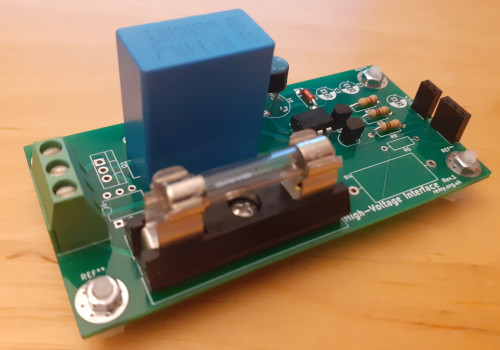
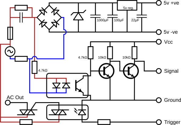
The circuit is a PCB version of the High-voltage interface used in many of the solid-state AC power control projects presented here in the past, coupled with what is a standard AC to DC power circuit. The most notable feature is the output from the power supply section (5v -ve and Ground) connections being separate from the power supply for the rest of the circuit, which was done because it provides the option this is intended as a multi-function board and some of that functionality requires full isolation between the high-voltage and low-voltage sides.
Power supply
With alternating current capacitors can act like resistors in that they limit the current flow, but in the process do not dissipate energy in the way that resistors do. With the current limited a zener diode is then used to limit the voltage to the desired level, and then this is further smoothed by other circuitry. This setup is known as a capacitive dropper and provides way to turn a high-voltage AC into lower voltage DC without a transformer. The effective resistance of the capacitor is due to reactance within the capacitor and the current flow is given by the following formula, whereI is current, V is voltage, f is frequency which is 50Hz in Europe, and C is capacitance of the capacitor.
I = 2πVfC
With 240-volt mains and a 0.68μF capacitor this works out at 51.3mA — capacitors rated for mains voltages tend to be big and expensive and this current seemed ample for the experimental nature of this project. The 470kΩ resistor is to ensure that dangerously high voltages will not be stored on the capacitor indefinately as it provides a path for discharge when mains power is disconnected. To avoid problem with inrush current there is a 100Ω resistor on the neutral side of the mains power input, although an ICL Thermistor can be used instead to reduce the amount of energy wasted via dissipation.
AC zero-crossing detection
The zero-crossing detection is present as an experiment to see if tapping off the AC active from between the current-limiting capacitor and the rectifier of the power supply would work as a way to avoid wasteful power dissipation with a zero-crossing circuit based around theH11AA1 when it is connected to 240-volt mains directly rather than through a step-down transformer.
Otherwise this part is a cut-down version of a previous AC power phase signal pre-processing system with the edge-to-impulse conversion removed, since the latter is only required for analog circuits rather than ones based around microcontrollers.
I had thought about using a buck converter instead of a linear voltage regulator but in the end decided not to overcomplicate the circuit.
Solid-state AC switching
The solid-state AC switching is a direct reimplementation of the isolated AC switching sub-circuit based around anMOC3021M optocoupler controlling a high-power triac, which has been used in many of the past projects on this site.
It is included because most projects that would require zero-crossing detection are power control circuits, and these days the marginal cost of fabricating a slightly larger PCB is very low so it makes sense to include this third function.
ICL (Inrush Current Limiting) Thermistors
Unlike normal thermisters that increase their resistance with temperature, inrush-limiting thermisters are a type of NTC (Negative Temperature Coefficient) thermister where resistance decreases with temperature, a property that is used to provide an initial resistance on power-up that then reduces as the device warms up. Of course it does not provide the same protection if a device is switched off then immediately switched on again, but it is a simple and cheap solution compared to active inrush limiting based around gating transistors. Compared to an inrush-limiting resistor it is pretty much a straight-substitution with the same data-sheet resistance rating.Creating the PCB
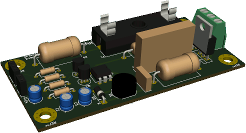
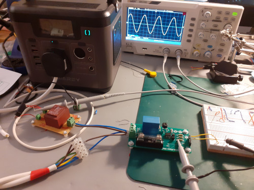
This is the first PCB I have made since the EEPROM programmer back in 2021, since I have for various reasons not been able to dedicate much time to electronics, and what time I have been able to I have preferred to use prototyping board. Hence this project was as much a shake-down of both my rusty design ability and a fresh installation of the software on my new(ish) workstation. At the time the PCB was designed KiCad 7 was just round the corner so I decided to stay with KiCad 5 for this circuit board and skip over KiCad 6 entirely. When laying out the PCB I had thought about adding in some provision for extra components but in practice whenever I have done this in the past they have ended up never being used, so here things are kept simple.
PCB fabrication
Fabrication was done by JLC-PCB who I used a lot back in 2018 and 2019 but mostly avoided in favour of Aisler during Covid lockdown due to problems with delivery, which included deliveries getting abandoned due to being stuck overseas. I opted for the cheap lead-based HASL process since this is a personal project for which I am going to be using lead solder with anyway, although annoyingly this low price is only for green PCBs and not any of the other colours. For those who need to be lead-free and only expect to use one or two of the PCBs, the Chinese fabrication services aren't that much cheaper any more and the saving is not worth the lead time. The board was ordered 30 December and arrived 12 January using the cheapest delivery option.

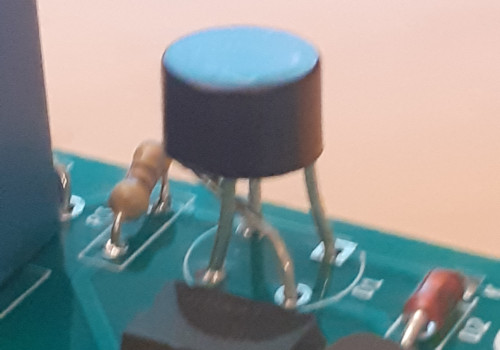
Perhaps a mistake or two was to be expected given how long it was since I last did a PCB fabrication design and order, but the number of errors made on this circuit can only be summed up as mega-cringe territory. I realised labels for the AC terminal block had been omitted almost as soon as I had sent in the gerber files and many of the components had incorrect PCB pads, most notably the pin-out for the bridge rectifier which was fixed by bending pins around as shown below. While there was nothing wrong with the board that could not be worked around it cannot really be described as a success.
Getting KiCad 5.1.12
For some reason KiCad have made it harder to find the older versions, which I suspect is due to a change of development systems rather than anything intentional, so below are the deep-links for the v5.1.12 release which was the last versions of KiCad 5. In Slackware 15.0 all the dependencies are now either a standard part of the distribution or have compatible versions in SlackBuilds so only KiCad itself needs building from tarball, but newer versions of some of the dependencies now have extra sub-dependencies. The development of KiCad has been accelerating ever since I first used KiCad 4 back in 2018 and I would not be surprised if I end up skipping straight from KiCad 5 to KiCad 8 or 9. These days I much prefer to use through-hole prototyping board whenever possible and for the time being I see no value in upgrading — it was almost two years between the last used KiCad for the EEPROM programmer and making this high-voltage board. Anyway there is a bug in v5.1.12 that causes lots of invalid regular expression errors such as the following:16:53:56: Invalid regular expression '^.*\gbr$': \g is not followed by a braced, angle-bracketed, or quoted name/number or by a plain number 16:53:56: Invalid regular expression '^.*\gbrjob$': \g is not followed by a braced, angle-bracketed, or quoted name/number or by a plain number 16:53:56: Invalid regular expression '^.*\pdf$': unknown property name after \P or \p 16:53:56: Invalid regular expression '^.*\pos$': unknown property name after \P or \p 16:53:56: Invalid regular expression '^.*\kicad_wks$': \k is not followed by a braced, angle-bracketed, or quoted name 16:53:56: Invalid regular expression '^.*\kicad_mod$': \k is not followed by a braced, angle-bracketed, or quoted name
No idea how this passed regression testing but it could be down to recent changes in how dependent libraries handle things. In any case the following patch snippet shows the problem, which is a missing dot causing the slash to treat the first letter of the extension itself as a special character. If there are problems with “Unknown error” messages, especially when trying to use 3D views, this is most likley due to wxWidgets being built to use GTK3 rather than GTK2.
--- kicad/tree_project_frame.cpp.orig +++ kicad/tree_project_frame.cpp @@ -545,7 +545,7 @@ if( i == TREE_GERBER ) // For gerber files, the official ext is gbr ext = "gbr"; - reg.Compile( wxString::FromAscii( "^.*\\" ) + ext + + reg.Compile( wxString::FromAscii( "^.*\\." ) + ext + wxString::FromAscii( "$" ), wxRE_ICASE ); if( reg.Matches( aName ) )
Circuit evaluation
The number of design mistakes meant that this circuit was not going to have its re-use value but the main purpose of making the PCB was experimentation, and on this front it was bit of a mixed bag but it is good to get back to doing this stuff after so long. In the past I have had electric shocks when testing high-voltage circuits so rather than using mains power I used a portable power source that I got a few months ago in preperation for rilling blackouts. It provides an isolated power supply that unlike mains is not referenced to ground, which is both safer and should not blow up the oscillscope via a ground loop should I poke a probe in the wrong place.
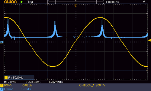
Capacitive dropper
I left out all the linear power regulation circuitry because I saw no point in populating it but that aside things worked as expected — the output voltage was the expected 6.2 reverse-voltage rating of the zener diode. Taking a look at the voltage across the bridge rectifier with an oscilloscope showed a rather interesting trace which is shown below; I can understand the dropper capacitor swinging between saturation voltages quite quickly but the circa 180° phase-shift I would be taking guesses at the cause of. The dropping capacitor was the only capacitor actually installed and there was no load on at time of measurement and this might account for the odd trace.
(Added December 2023): This circuit was made before I properly understood the phase-shifting with capacative and inductive loads compared to resistive loads. The process of charging up the dropping capacitor introduces a delay before the ‘output’ side reaches line-voltage and hence phase-shifts the AC wave-form, which in hindsight should have been obvious having previously used series capacitors to delay pulses within DC circuits.
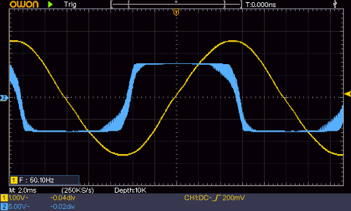
Crossing detection
Having aH11AA1 crossing detection opto-triac downstream from a capacitive dropper simply did not work out, as can be seen in the oscillopscope plot below where the input power is in yellow — which has been stepped down to 5 volts using an isolation transformer — and the opto-coupler output in blue.
I tried different values of resistors on the AC side of the opto-coupler but was unable to get any output that could be considered useful, being both a weak signal and if anything marking the peaks of the mains wave-form rather than the zero-crossings.
I have the suspicion there may be other things wrong with the circuit but saw no value in investigating further.
This is problematic because it means a step-down transformer is needed for situations where zero-crossing synchronisation is needed, which defeats the whole point of using a capacitive dropper in the first place in order to avoid the use of transformers. In most cases once the bridge of having a transformer for the zero-crossing detection is needed, it makes more sense to size it to power the whole circuit rather than relying on seperate circuitry.
Power control
The order of a new stock of WeenBT136 high-power traics did not arrive in time so the AC power output part of the circuit was never tested, but since it followed a design I had used in the past it is unlikley it would have had any problems.
In this circuit it was something of a tag-along and is only really suitable for resistive loads since it does not include any snubbing, the latter being something I need to investigate should I ever have the need to switch inductive loads.