Hard-wired triac control, 2nd gen.
03 January 2021This circuit is a second iteration of my previous hard-wired triac control circuit because I felt that it was better to start over rather than try to fix all the faults with the latter. The circuits provides an I2C-interfaced power-control that as the name suggests used hard-wired circuitry rather than use of a micro-controller like I did with my first solid-state control circuit. Unlike the previous triac-based control circuits this one was built from the outset with access to proper test equipment.
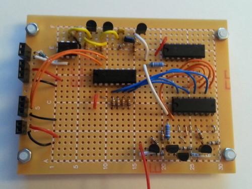
The basic idea behind this system is the same as the the previous iteration of the circuit, which in summary is to emit pulses that are aligned with the crossing-point of AC power cycles, which in turn trigger a triac that controls the output mains power. The various control signals are summerised in the diagram below — finer details are in the previous articles.
Circuit sub-systems
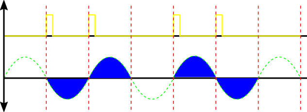
The underlying concepts and the overall sub-systems are much the same as the previous iteration, although this time round I decided to revert back to the MulticompMC01010 prototyping board and have the circuit on a single board — I think this particular board is from some stock I bought back in 2017 or 2018.
I found that someone had made some smaller-sized resistors for Fritzing so the breadboard in Fritzing reflects the actual circuit quite well, so the former is shown below.
The one thing that the previous circuit has but this one omits is the triac itself.
AC power isolation
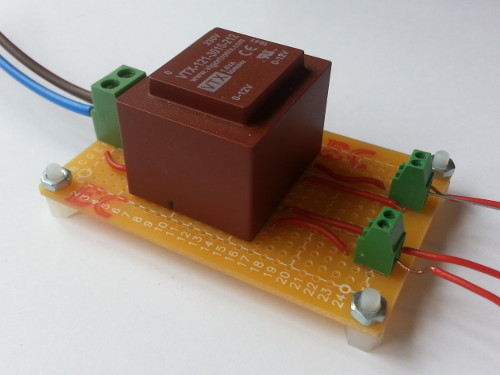
I got two or three electric shocks while probing the previous generation circuit so I decided that having full 240-volt mains on prototyping board was simply too dangerous, and in addition was not comfortable with huge resistors dissipating several watts. As a result I decided that I would step down the mains AC voltage using an isolation transformer mounted on a separate board, and this board is shown below — originally I made it so that I could get a clean mains AC signal on my oscilloscope, although it was not quite as clean as I was expecting. For safety reasons I also did not include the high-voltage switching sub-system in this iteration of the circuit.
Phase signal pre-processing
Pre-processing of the phase signal to obtain a well-defined square pulse is something that was discussed in the first-generation circuit article, although I decided to use a different sub-circuit that avoided doing fancy things with negative voltages, and the schematic for it is shown below. The first transistorQ1 turns the pulse from the H11AA1 into a nice sharp square wave;
Q1 inverts the wave;
the capacitor approximately takes the derivative of the square wave, which amounts to a positive impulse for the rising edge and a negative impulse for the falling edge — the latter is filtered out by diode D1;
and the final transistor Q3 inverts the active-high impulse, turning it into an active-low square shape.
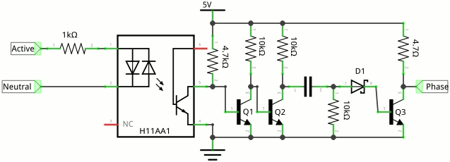
Using a 47nF capacitor results in the phase signal pulse being about 1ms, and I expect this width to also be affected at the very least by the pull-up resistor to the left of the capacitor. I had considered adding a buffer to end of this sub-system, and if so it would have been based around a 555 chip, but in the end decided that it was not necessary.
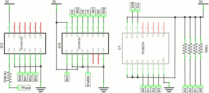
Phase counting sub-system
This sub-circuit generates the enable signal based on a 4-bit counter that wraps around, and is virtually identical to the triggering sub-system in the previous project revision. The one addition is the 78.8kΩ resisitor on theSV74HC393 cotuner's clock input because it looks like this pin is not high-impedence and adding the external resistance made certain problems disappear.
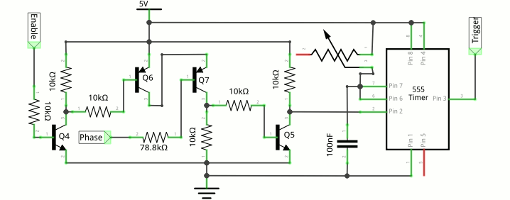
Trigger pulse generation
Unlike other sub-systems the pulse generation from the previous project has been significantly redesigned. TransistorQ4 changes the enable signal from active-high to active-low to make it the same sense as the phase signal, and the other three transistors form a NOR-gate that outputs an active-low signal for the 555 timer's trigger pin — not to be confused with the trigger signal that is output.
The variable resisitor was to allow adjustment of the output trigger pulse duration.
Experimentation
Unlike the previous version I had access to an oscilloscope for the entire duration of this project, and the testing presented here was done in parallel to designing & building the circuit. In fact this project was as much an excuse to make proper use of this equipment as a desire to create an operational circuit. All the traces were taken using the oscilloscope's save functionality, although they have all been edited to varying extents, mainly to reduce physical size.
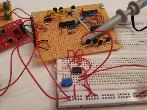
As can be seen from the picture above the 555 timer part of the trigger pulse generation was omitted from the main circuit and was instead mounted on solderless breadboard —this is explained in the remarks section.
Opto-coupler AC current
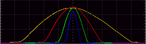
The photo-coupler is rather more complex than I originally thought it was, and to me it looks like it has a fair amount of capacitive behaviour. In the first-generation board the output pulse from theH11AA1 was rather wide, and since the measured forward current on the AC side of 3-4mA is significantly below the 10mA that the data-sheet characteristics section assumes decided to try various values of current-limiting resistor to see how forward current affected the profile of the pulse.
The results are shown in the composite oscilloscope plot below — from widest to narrowest the traces correspond to 3mA (yellow), 6mA (red), 12mA (green), and 24mA (blue).
Using the 10mA suggested by the data-sheet significantly sharpened up the pulse, but it was clearly diminishing returns going much higher.
For the 12mA & 24mA tests that used 10kΩ resistors they were getting noticeably hot and then I realised that at 230 volts even these notionally low currents add up to quite a significant power dissipation. The 10kΩ resistors used for these two currents were rated for one watt but I really needed something rated for three watts, and I suspected such components would be huge. I re-ran the experiment with the voltage stepped down to 12 volts and these results are shown below; the traces are 0.92mA (yellow), 3.68mA (red), 9mA (green), and 32mA (blue).
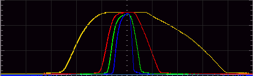
With 12 volts the narrowing occurs at a lower current but as with 240 volts there still seems no real value in going higher than 10mA.
In hindsight I do wonder whether the pre-processing of the above was strictly necessary, but it at least made things easier to measure.
Phase signal lead
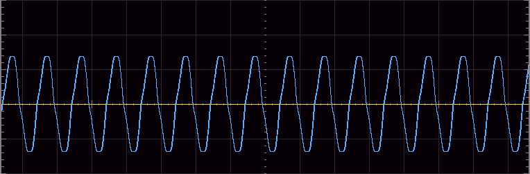
One of the most important quantitative factors in the whole circuit is where the phase signal pulse comes in relation to the actual AC power crossing point, and this is shown in the oscilloscope trace below.
By zooming in it can be seen that the falling edge is 120μS before the zero-crossing point, which is not surprising because the emitter within the optocoupler stops emitting just before the crossing is reached. The pulse itself is about 800μS,.
The rising edge is not quite as sharp as the falling edge, which is one of the reasons I thought about adding a Schmitt trigger to the pre-processing sub-system.
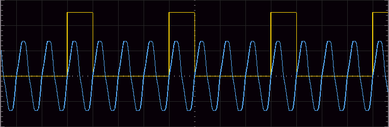
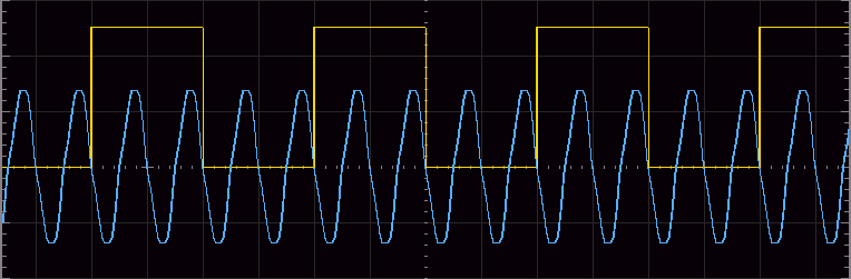
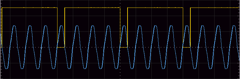
Enable signal
In the previous revision of the circuit I had issues with the phase counting, so for this revision it is something I checked before building the rest of the circuit. The four graphs below show the enable signal in relation to the input AC power wave-form for different power levels, going from “off” to “full power”. One notable thing is that the full power trace still has one half-cycle switched off, which is an artefact of how the enable signal is generated, which was detailed in a previous article on the duty-cycle resolution.
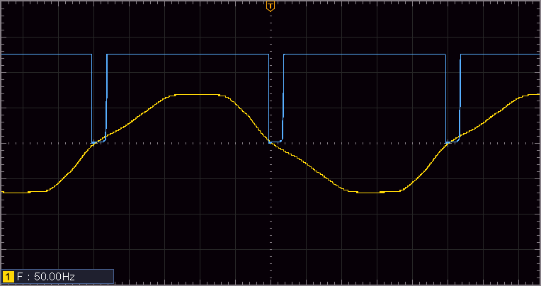
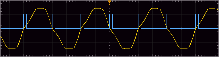
Trigger signal output
The all-important signal is ultimately the trigger signal that is connected to the triac, and this is the external output for this circuit. This signal is shown in the oscilloscope trace below alongside the input mains power wave-form, and this represents the successful end-to-end operation of this control circuit. The trigger pulse is 100μS ahead of the zero-crossing, which is slightly less than the 120μS observed with the pre-processed phase signal, which I assume is due to propagation delays; the trigger pulse itself is 1ms, and since this is not much above the 800μS of the phase signal pulse is close to the smallest pulse the circuit will support.
Remarks
This revision of the circuit was successful in that it did not have the issues the previous one did, although some new issues did occur which meant that the power control would not be quite as good as expected. Nevertheless the issues are minor and fundamentally the circuit does what I wanted it to. It required more components than I planned, with sub-systems built on solderless breadboard first, but this project was as much about process as outcome. I left quite a few things out of the scope of this revision, and these are detailed alongside other issues below.SN74HC393 counter chip oddities
I thought theSN74HC393 counter was clocked on the rising edge when in reality it is clocked on both the rising and the falling edge, and this has two effects.
Firstly the least significant output bit from the counter is the inverse of the clock so that it is always the same value at the time the enable signal is required, which means one bit of power-level granularity is lost — this can be seen in the enable signal traces.
Also in the case of the falling edge I suspect there is a race condition between the phase signal counting updating the enable signal and the trigger pulse generation emitting a trigger pulse for the triac, as the first pulse in the “on” window of time is sometimes missing. Using an alternative such as the CD4510BE which is only clocked on the rising edge should avoid both of these issues.