AC power control, 3rd gen.
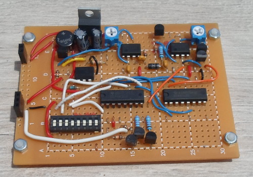
09 May 2021This circuit is an incremental development of my previous “hard-wired” triac control circuit, which in turn is part of an on-going series of AC power control circuits in which I deliberately use hard-wired electronics rather than relying on firmware. Although this revision does also include some simplifications compared to the previous circuit, the real focus is fundamentally about introducing analogue phase-shifting and trigger pulse width controls. The finished circuit is shown below on prototyping board, and this was a circuit built in the knowledge that it would very likely be the last serious electronics I would do for some considerable time.
For convenience I decided from the start to have an on-board AC-to-DC conversion sub-system rather then relying on an external regulated DC power supply, and it is assumed that for safety reasons the mains AC power that acts as both circuit power and phase reference has been stepped down. I also replaced the I2C-controlled I/O expander with DIP-switches because it made testing of what was still a circuit intended for experimentation a lot easier since I did not need to have something to act as an I2C master at my workbench.
Circuit design
The overall design of the circuit is shown in the schematic below. Power for the circuit comes from conversion of AC to DC and the top-left part of the schematic shows the sub-system that perform this — it consists of a bridge rectifier that then feeds a regulation circuit consisting of smoothing capacitors and a linear voltage regulator. The rest of the circuit consists of several stages of mostly analogue signal processing, which are described subsequently.
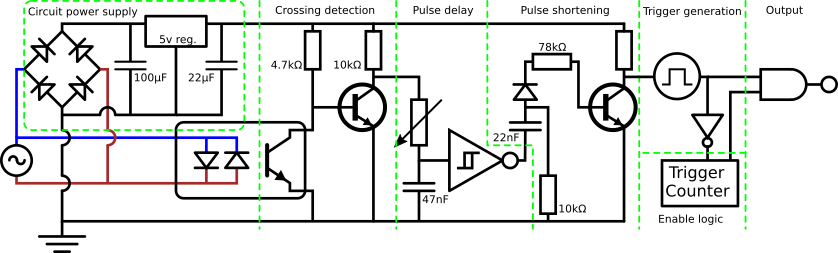
- Crossing detection
- The
H11AA1opto-coupler detects zero-crossings of the input AC power supply, and the open-collector output of this is used to control a current-sinking NPN transistor that turns the phase-crossing pulse into a sharply-defined square wave. The latter is not strictly necessary but it was done for ease of trouble-shooting, isolating the rest of the circuit from any oddities of the photo-transistor. - Pulse delay
- The output of the crossing detection is ahead of the actual zero-crossing, so a combination of a simple resistor-capacitor and a Schmitt trigger is used to introduce some delay into the circuit. The variable resistor affects how long it takes for the capacitor to reach the Schmitt trigger's threshold, which allows for about 800μS of adjustment. The Schmitt trigger itself is implemented using a 555 timer chip since there are not really any other options for through-hole circuits.
- Pulse shortening
- Again this is a processing stage could be omitted, but the width of the pulse at this stage is a lower-bound on the width of the eventual trigger signal, and I felt that this lower bound was too high. A blocking capacitor together with an output pull-down resistor integrates the square wave into impulses, and a diode is used to block the negative impulse resulting from the falling edge. This then controls a current-sinking NPN transistor that turns the positive impulse back into a square wave. The latter is active-low but this inversion is reversed in the next stage.
- Trigger generation
- A 555 timer wired for monostable operation with a variable resistor is used to allow the width of the pulse to be varied between 300μS and 2.2mS, and the output is the trigger signal that is adjusted to match the timing requirements of the circuit output. In order to avoid instability with the enable logic, this trigger signal is inverted before being passed to the phase counting logic so that increments — and hence any change in the enable signal — occur on the falling edge of the trigger signal.
- Enable logic
- Described later in more detail. This counts trigger pulses and compares the count to a preset value, which in turn controls the enable signal that allows the trigger pulse to be passed on to the output.
Output enable logic
The circuitry to decide whether to assert the enable signal is based around having a counter that increments and then wraps around back to zero, and a comparator that asserts the enable signal while the counter is below the reference value of DIP switches. The wiring is shown in the schematic below.
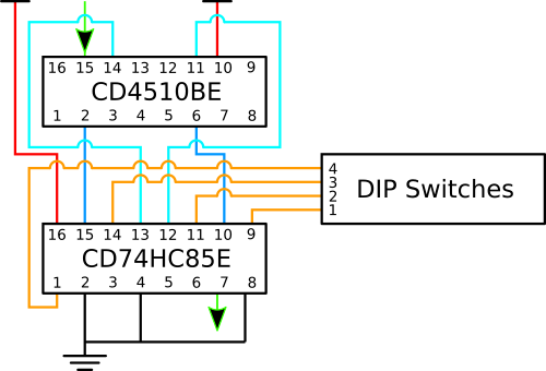
I used a binary-coded decimal counter that wraps around back to zero after 0x9 rather than the 0xf that a true binary counter would wrap around at.
A consequence of this is that there are only eleven power levels rather than fifteen, making five power setting redundant as anything above 0xa on the DIP switch is always above any value the counter will present, but as an intentional side-effect available power levels include both fully-off and fully-on.
Transistor-based logic
For reasons of space the AND & NOT gates in the circuit are built using transistors. From the start the NOT gate that inverts the trigger signal before it is input into the phase counting logic was always intended to be the complimentary pair of MOSFETs shown below. This combination is very compact slotting conveniently into the top-right corner of the circuit, with the high-impedence input of MOSFETs negating the need for any resisitors.

However the AND gate which generates the final output based on the enable and trigger signals was originally done using an integrated circuit logic chip, but for various reasons there was not the space left for this chip on the prototyping board so it was replaced with the transistor-based circuit shown below. This is actually a NAND gate followed by a NOT gate, as with this combination the voltage corresponding to a high output is close to Vcc.

Prototyping the circuit
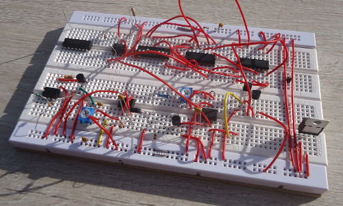
Since a significant portion of this project was experimenting with various combinations of components to get the effects I wanted, the circuit was initially built on solderless breadboard and this is shown in the picture below. This was to allow easy swapping in and out of components for a circuit that was evolved rather than designed. The result was not quite the same as the final one on soldered prototyping board, most notably the absence of the AC-to-DC power conversion and the use of a chip rather than a transistor-built AND gate for the final output. The board is actually two breadboards put together and then stuck down to plywood, which I found to be much more cost-effective than a larger off-the-shelf breadboard.
Circuit output
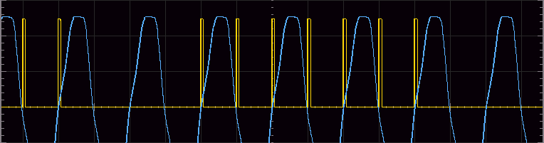
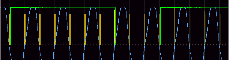
The oscilloscope trace below shows the input AC power in blue and the circuit output in yellow for a 70% power setting, where seven of every ten half-waves get activated. This latter output signal would in turn be connected to an external circuit that has a Triac that switches the mains power being controlled, and this worked with the test rig I used with previous iterations of the control circuit. Notably absent are artefacts that were present on the traces from previous circuits.