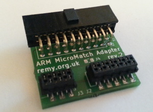
MicroMatch ARM adapter respin
12 April 2020This is a redesign of my previous MicroMaTch ARM adapter which in turn was made in response to the disproportionately high price of receptacles needed for standard JTAG connectors — a 10-pin mini-IDC was the best part of €3 whereas an equivalent MicroMaTch was around the 60¢ mark. Following on from the Kinetis KE04 breakout board that made use of this adapter I decided to make an updated version that took account of changing requirements. This adapter is also a first for me in that I have decided to open-source the hardware design for the PCB.
Revision considerations
In making a second revision of this adapter there are four specification changes I thought about and these are detailed below; two of them I took on board as an improvement and two I rejected as likley to cause more problems than it would solve.- Programming pin-outs
- Apart from the ST Micro Cortex-M4 board I have always used SWD (Serial Wire Debugging) for ARM chip programming, albeit in the case of my first NXP USB tryout it was due to issues with OpenOCD not supporting full JTAG. A six-pin connector is the smallest that could accommodate the five connections required for SWD, and this was used on my KE04 breakout board. However it is a different story with the eight-pin connector which I have decided to drop in favour of a ten-pin connector using “official” JTAG pinning. If space was actually an issue I would always opt for the six-pin SWD connector.
- Programmer-supplied power
- I had thought about whether to have the adapter board itself supply power, which would be useful for the reprogramming on daughter-boards that may typically be removed from their host for the operation. However I soon concluded that it was better to keep things simple and have the adapter do just one task — this redesign is all about improving the board based on practical use, and adding extra functionality speculatively would detract from this goal.
- Connector orientation
- The first revision of my MicroMaTch adapter had an unpolarised IDC connector soldered from the bottom of the PCB rather than the top, which in itself was a bodge fix carried over from an even earlier flash connector I had made. Having now managed to source some polarised connectors I decided to do away with this idiosyncrasy.
- Removing the clock jumper
- When looking at JTAG schematics there was always provision for a jumper between pins 9 & 11 — the transmit and receive clocks respectively — which I never really understood. In practice I never saw the need to tie these pins together, but the lack of understanding made me reluctant to eliminate the jumper entirely. As a compromise I changed the jumper footprint to an 0805 SMD resistor pad.
PCB production
Since this was a small PCB I ordered it from Aisler purely for the fast turn-around time, and although they took longer than expected to fabricate the board the shipping time was faster than usual — shipped on Wednesday and found it in my letter-box on Friday. The PCB arrived just before the weekend I was due to move to a new apartment so I quickly reflowed the surface-mount connectors before packing things up and added the through-hole connector later. The connector part numbers are given in the table below:
| Description | Vendor | Part number | Vendor | Order code |
| 6-pin SMD MicroMaTch | TE Connectivity | 2178711-6 |
Farnell | 2473358 |
| 8-pin SMD MicroMaTch | 2178711-8 |
2473359 |
||
| 20-pin polarised right-angle IDC | Valcon | B07a-20-AGA1-G |
Toby Electronics | B07a-20-AGA1-G |
Right-angled polarised IDC connectors were surprisingly difficult to source — finding a suitable connector was one thing but then there was the problem of finding a vendor who would supply connectors in suitable quantities. Manufacturers themselves are only interested in bulk orders in the thousands but they tended not to list down-stream vendors for those only wanting a dozen or so.
Reflowing the MicroMaTch connectors
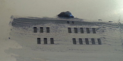
I decided to do the reflow before moving out because it meant I was using a hot-plate I had previous experence with. The process I used for reflow soldering the MicroMaTch connectors is the hot-plate method covered in a previous article although for this PCB there are two significant differences — I used the Chip Kwik solder paste almost straight out of the fridge rather than allowing the recommended 4 or so hours for it to reach room temperature as I suspected it being a bit more viscous would make things a touch easier; and the excess paste was scraped off as shown below so that the quantity that ended up on the landing pads was just the thickness of the solder stencil.
The paste I used was well beyond its notional shelf life, although I did keep it refrigerated in an air-tight box with a bag of drying agent, and with the caveat of not having done much reflowing recently I did not notice any degradation in its performance. Old stock might be an issue with finer width landings but without a using old & new stock together I cannot be certain. I recorded the reflow process on my microscope and the clip below shows the point that the paste melts and capillary action happens:
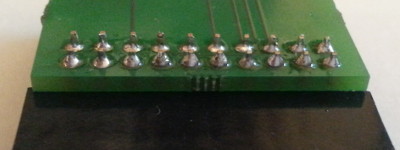
Through-hole IDC connector
Nothing special here but due to circumstances I soldered on the IDC connector this weekend rather than at the time I reflowed the SMD connectors. Rather than my usual soldering station I used a portable soldering iron I bought from Maplin, which although got the job done is a bit irritating to use. Being powered by AA batteries it takes a while to heat up but otherwise the biggest irritation I found was the shape that required holding the iron in a way that I was not used to while soldering.
I had a stock of lead-free solder from my previous comparison but since I was not sure where it was packed away I opted for my usual lead-based solder — my impression of lead-free solder is not good anyway so I would likley only use it for things I planned to give to others. The soldering iron was made for lead-free solder which requires higher temperatures, which might explain why I found no problem getting the solder to melt.
MicroMaTch specification issues
A major flaw with the MicroMaTch series as a whole is that the technical drawings do not actually state what the pin numbering should be. Ribbon cable markings do the intuitive thing of putting the Pin 1 wire colouring the same side as the polarisation leg, and this convention of using the notch as the Pin 1 marker was used with my original adapter, but for some reason KiCad's MicroMaTch footprint generator puts the polarisation notch at the opposite end of the landing to Pin 1 as shown below. I am not sure why I did not notice it before and I am thankful that the ARM programmer I use has protection against miswiring.
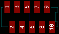
I have no idea which way round is officially correct but despite it being counter-intuitive I am going with what KiCad thinks is correct — without anything more authoritative this seems the best option since KiCad is the only tool I use for creating PCB designs these days. Had I been aware of these issues up-front I have doubts whether I would have opted for this connector series but the investment is now a sunk cost.
PCB design files
While I have in the past published schematics for circuits I have made, for this circuit I have made public all the files required to fabricate the PCB, and doing this with a relatively simple circuit allowed me to figure out the best way of making them public. Originally I was going to just provide ZIP files but thinking back to when I moved software projects across to Bitbucket I felt that this would be asking for trouble, so in the end the approach I opted for is the same that I used for firmware — a single repository on Bitbucket with designs in sub-directories. This is a method of presentation better suited to Subversion but I felt that having a repository per PCB would be too much of a logistical headache to keep in sync with my own computer. The repository includes all the KiCad project files, as well as footprints for through-hole MicroMaTch connectors, in addiiton to Gerber exports ready for fabrication. The repository includes its own Readme file which is a living document that should be consulted for any changes made since this article was published.In the repository is a third revision of the adapter which has cosmetic changes compared to the one used for fabrication of the PCB presented in this article. The only practical change is text on the silk-screens — notably calling it a JTAG adapter rather than a ARM-specific adapter — although I did make behind-the-scenes changes such as the naming scheme used for footprints. One addition which is not used on the PCB itself is a footprint for the through-hole connector that has the same pin numbering as the surface-mount connectors. I am undecided what licence to use for these design files but at the very least I am happy for the average Jo Public to submit them as-is to a fabrication service in order for them to get a copy of the PCB for their own use. People wanting to mass-fabricate the design and flog it on E-Bay is another issue though.