Reflow soldering
14 March 2020This is not the first time I have used reflow soldering with surface-mount components but it is the first time I have reflowed all the surface-mount components on a PCB that was not a simple break-out board. I also decided to take the opportunity to better document the reflow procure I use because time commitments means it is unlikely I will use the board in the near future. The circuit itself is a follow-up of my previous LPC11Uxx USB try-out but the underlying purpose is beyond the scope of this article. In summary I used Chip-Kwik Tin-Bismuth solder paste which I applied using a solder stencil and then reflowed using a hot-plate. Some rework was required but at the end I had an operational board.
Applying the solder paste
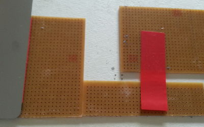
The one messy part of reflow soldering is putting down the solder paste, and in this case a solder mask is used. I use the mounting board shown in the picture below to hold the PCB in place — the bits of perf-board are the same thickness as the PCB, with the pieces to the left and bottom are glued to the base-board, whereas the piece to the right is loose. The PCB is places in the gap in the middle, and the loose piece of perf-board is taped down in order to clamp the PCB.
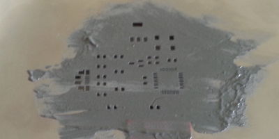
The solder paste mask is aligned over the PCB and once in the correct place it is also secured using tape. At this point the solder paste is spread over the top of the mask as shown below — in this case the mask bends up a bit so it needs to be held down in place while applying the paste. In this case the layer of solder paste is actually too thick but it demonstrates what is going on — the paste should just be in the gaps and the excess paste on top scraped away, as the thickness of the solder mask is such to leave just the right amount on the PCB.
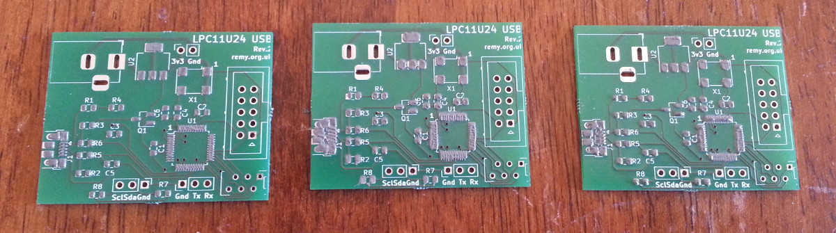
I laid down the solder paste for three PCBs and these are shown in the picture below. I feel that the one on the far left has the right amount of solder paste whereas the other two have clearly far too much, although this only really matters for the four-sided LQFP chip and the Micro-USB connector on the left-hand edge.
(click to zoom)
Placing the components
Once the solder paste has been laid the next stage is to put down the surface-mount components, as shown in the picture below. Note thatR3, R7, & R8 have been left empty and the solder paste for these pads has been wiped away.
A slight misalignment of components does not matter as capillary action will pull these into place during the reflow process, although C4 is at the limit of what I would consider to be tolerable misalignment.
I used some Duratool 1PK-104T-F right-angled tweezers for placing the components, which although are great for the smaller passive components are a bit of a pain for chips due to having a poor grip. Although I did not have it at hand at the time I did this reflow a tool I have in the past found much better for placing surface-mount chips is the Duratool D00769
vacuum pickup tool.
Doing the reflow
For the reflow itself I use the hot-plate method which involves placing a metal plate on top of the hob, and then putting the PCBs on top of this plate as shown in the picture below — I have in the past put PCBs directly onto the hob but I do not recommend doing so. The metal plate helps distribute the heat from the hot-plate, as well as keeping any grease that might happen to be on the hob itself off the under-side of the PCB. I use an infra-red heat sensor to measure the temperature although in practice it is easier to simply watch the solder paste melt and flow into position than to try approximating the reflow charts provided on data-sheets.
Only real rule-of-thumb is to turn the hob down once the chip itself is close to the solder paste melting temperature, as the hob itself will already be about 100°C hotter due to the lag the steel plate introduces. The process is a bit of an art due to the nature of the heat source used.
The soldered board
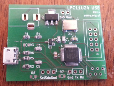
When removing the reflowed PCB from the hot-plate, care must be taken not to knock components out of place before the solder has solidified — the best thing to do is put them down somewhere near the hot-plate and leave them there until the board has cooled down. This should only take a few minutes but in doubt leave it that bit longer, particularly as a board where the solder has solidified may still be too hot to handle by hand. The picture below shows one of the newly-reflowed PCBs.
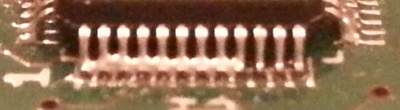
Note how all the components are now straight even though they were not just prior to the reflow heating. There are obvious solder-bridges on the microcontroller but this is a common occurance that is corrected later.
Board rework
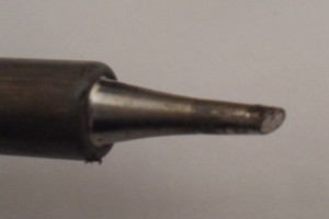
Sometimes a PCB is ready to use once the reflow process is complete but in this case further rework is required to correct defects that are introduced as part of the soldering process. In this case the problem is solder bridges which is a short-circuit between neighbouring solder pins. This is most obvious on the LQFP chip but a close look at USB connectorJ1 also reveals such a short. These need to be removed by hand using a soldering station although the process does vary a lot. A few solder bridges disappear with just a bit of heat from a soldering iron tip and many more can be swept away in a single stroke after applying some flux, but from my experience there is always at least one that requires excess solder to be sucked up using desoldering braid — for the latter I use Loctite NC-BB. I have sometimes found that a flat-hoof soldering tip such as the T18-C2 shown below is much better for rework than the standard pointy tip.
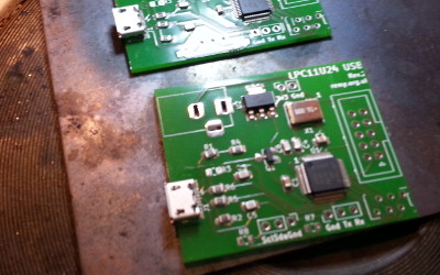
One of the three PCBs had reflow flaws that went beyond just solder bridging and this one is shown in the picture below. In this case the pins of the microcontroller have become misaligned and ended up halfway between the pads they were supposed to be on, due to the chip moving too far to the left. In this case much more drastic rework is required as at the very least the solder on all four sides will need to be melted to allow the whole chip to be moved into the correct position. While I do have a hot-air reworking station that would be suited for such a task reworking this particular chip is something for the future.