Hard-wired triac power control
05 December 2020This is a follow-on from my hard-wired duty-cycle counter and it is a hardware-only version of what was previously done entirely by firmware — counting phases and deciding which AC mains half-waves were switched on for power control purposes. The power level setting is specified via I2C using an I/O Expander, the motive being that I want a daughter-board that just needs to be populated rather than having to flash a firmware as well. This article will mostly cover the theory as I have not had the opportunity for proper testing.
Circuit design
Although based on the previous solid-state AC control and duty-cycle counter this circuit is a simplification for which reduction in the number of chips required was a major design goal. One effect of the aim for simplicity is that power control is only at the granularity of switching on and off entire half-waves and the graph below summarises the control signalling for an illustrative 2:3 power load (i.e. 66% duty cycle). The input AC power which is shown as a green line and from this phase alignment impulses shown by the dashed red lines are used to synchronise the control signal, the latter which is shown in yellow. The control signal is used to trigger — or not — the switching on of each half-wave of AC power, with the half-waves switched on indicated in blue.
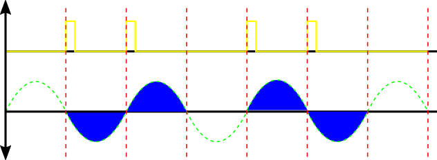
Since the signal pulse only needs to be at long enough for the triac that switches the AC output to trigger, and this pulse is itself syncrinised by the the AC input itself, the circuit does not have any tight timing requirements. It just needs to count the half-waves and based on this decide whether to let the phase detection pulse propagate to the triac circuitry. While finer-grained power control can be obtained by chopping up the half-waves doing this property would mean needing to detect the main frequency and hence the half-wave width, and then using this to derive a delay for the trigger pulse — doing this with hard-wired electronics rather the firmware
Duty-cycle counter resolution
My original plan was to have both the high and low portions of the duty cycle as independent 8-bit values but to get around some edge cases I switched to having one that defines the high portion and the second defining the width of the whole pulse wave. One effect of having two parameters is that a given power settings can be obtained using many different value pairs, so I favoured minimising the pulse wave period and before long realised that in most cases the period was only using 5 bits. As a result I decided to limit myself to 4 bits as I felt that the increments in power level this would cater for, as indicated in the table below, would be adequate for my heating-control use-case. Since the less-than comparator signal is used to gate the triac triggering, the last half-wave is always off, so 100% power cannot be obtained.
| Switch-off value |
Power level (vs. period) | |||
| 4-bit | 3-bit | 2-bit | 1-bit | |
| 0 | Off | |||
| 1 | 6.25% | 12.5% | 25% | 50% |
| 2 | 12.50% | 25.0% | 50% | |
| 3 | 18.75% | 37.5% | 75% | |
| 4 | 25.00% | 50% | ||
| 5 | 31.25% | 62.5% | ||
| 6 | 37.50% | 75% | ||
| 7 | 43.75% | 87% | ||
| 8 | 50.00% | |||
| 9 | 56.25% | |||
| 10 | 82.50% | |||
| 11 | 68.75% | |||
| 12 | 75.00% | |||
| 13 | 81.25% | |||
| 14 | 87.50% | |||
| 15 | 93.75% | |||
At some point I am going to do experiments to find out how power level translates into temperature rise, and the transients when the power level is changed. As for the period rather than having a second comparator to trigger the counter reset I decided to simply let the counter wrap around, since with 4 bits at 50Hz mains (i.e. 100 half-waves a second) the maximum control cycle period is only 160mS and I saw no real benefit in trying to shorten this. Cases where this matters are probably ones where I should be chopping up the half-waves rather than only passing complete ones.
High/low voltage interface
This is the phase-detection and power-switching from my original solid-state power control circuit, the only significant change being the increased resistance due to theH11AA1 being connected to the 240-volt mains directly rather than the output of a step-down transformer. All the high-voltage parts of the circuit is entirely within this section and there is optical isolation between the high and low voltage wiring.
It has the phase detection as an output signal and the triac triggering signal as input.
The MOC3021M has a maximum LED forward voltage of 1.5 volts and a maximum trigger current of 15mA, which with a 5-volt supply rail is obtained with a protective resistor of 233Ω.
220Ω is used as it is the closest I could find — I previously used 1kΩ so I am guessing the specified 15mA threshold is extremely generous.
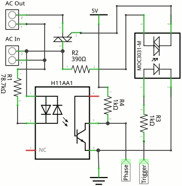
The schematic has had some manual editing in Gimp — the H11AA1 actually used the 4N35 as a placeholder which has an identical pin-out but the LED input is polarised, so I changed the image to show a second LED in the reverse direction.
Fritzing has a triac symbol but it had a different pin-out to the BT136-600D so I originally built the circuit using a voltage regulator as a substitute since it had the same TO-220 package, but later I worked out how to make a custom component that had the correct pin-out.
There is no symbol for the MOC3021-M so I used the zero-crossing variant MOC3031-M which is virtually identical.
Half-wave triggering sub-system
The purpose of this sub-system is upon receiving a phase signal pulse to decide whether the half-wave should be switched on or off. In the previous solid-state switching circuit this was done by an interrupt handler within the firmware so to be a viable alternative to just using a microcontroller it had to undergo a lot of simplification. Rather than DIP switches the comparator input uses aPCF8574 I/O Expander coupled with pull-ups to account for the latter having open-drain outputs, and as a result the duty-cycle is controlled via I2C.
I recently evaluated the NXP PCA9536 which is a 4-bit I/O Expander with driven outputs rather than open-drain in an 8-pin package, which would take up significantly less space but it is not available as a DIP package.
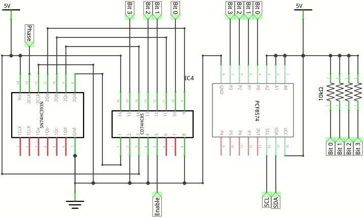
Fritzing actually had a symbol for the PCF8574 but it is not any different to the generic integrated circuit the other two components use.
Incidentally it is circuits like this that using labels rather than drawing out all the wires is very useful, but this is something I only realised was supported by Fritzing once I was already close to stopping using it.
Trigger pulse generation There are two signals that play a part in emitting a triac triggering pulse — phase synchronisation and whether the half-wave is one that should be switched on, and the actual pulse generation is done using a 555 timer. Since the 555 in a monostable setup has an active-low trigger, a NAND gate built from two NPN transistors is used to create the activation signal, and the time-constant of the 555 dictates how long the trigger pulse should be. A 12kΩ resistor and 0.1pF capacitor results in a pulse of 1.3ms which is approximately double the 786μs that previous experimentation suggests is needed to guarantee that the triac activates.
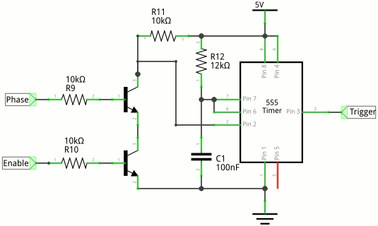
While the 555 is predictably a built-in component in Fritzing I would have preferred if they had named the pins rather than numbering them. I did have some dedicated NAND chips in stock but I felt it would be a little wasteful to use just one of the four NAND gates each chip carries. In hindsight I think it would have been better to use it anyway.
Pulse generator calculation
Pulse generation is the standard 555 monostable setup where the width of the pulse is Ln(3)*R*C and below is a Javascript snippet that can be used to calculate this equation. It is based on my previous astable period & duty cycle calculator.
| Component | Value | Units | |||
| Resistor R | |||||
| Capacitor C | |||||
| Pulse width | 1.0mSec | ||||
Breadboard layout tools
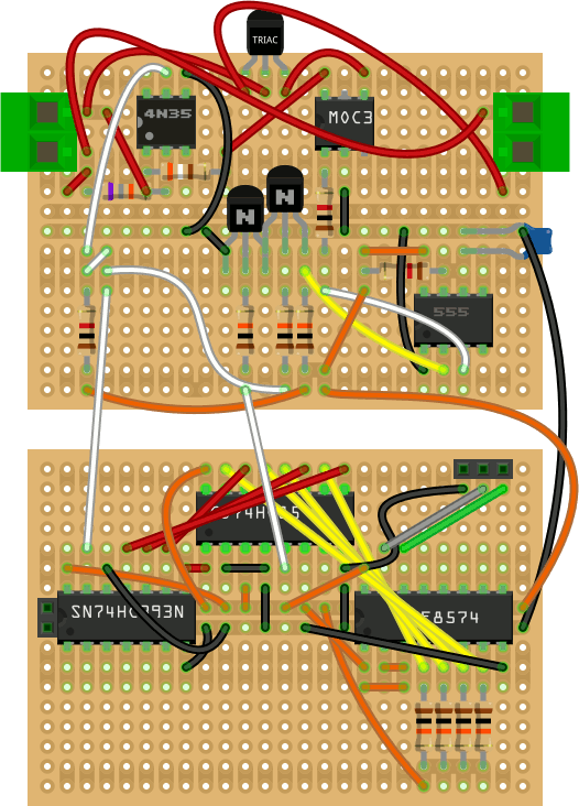
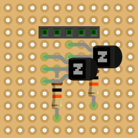
It has been a long time since I last used Fritzing but after much searching for tools to help with laying out circuits on breadboard I came to the conclusion is was pretty much the best thing going. For PCB work it is really a training program and especially with designs involving surface-mount components it is basically not up to scratch but it is a huge help with anything on prototyping board — this is especially true with strip-board which needs advance planning on where to cut tracks and the most notable example is the 17-segment LED display now used for the website banner. The completed breadboard view in Fritzing, as it was prior to me starting to build the actual circuit, is shown below.
To be fair even for this circuit I discovered some features of Fritzing that had I known about in the past I probably would have used it a lot more, although I doubt I will ever use it again to produce a PCB as for the latter KiCAD is simply miles better. The next sub-sections summerise the areas where Fritzing is actually very annoying.
Occlusion by components
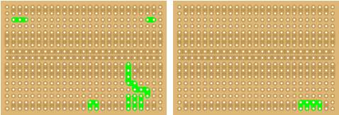
One major irritation is the perspective projection of many components which covers up more of the circuit than it needs to, and this makes it very difficult to use Fritzing to lay out high-density circuits. Integrated circuits and resistors are fine because they are flat, but other components such as transistors and capacitors have a perspective projection that hides part of the surrounding board. This is best illustrated by the two images below, one of which is Fritzing's breadboard view, and the other is the components laid out on an actual perf-board.
New components
Fritzing is notorious for making it very difficult to create new components and this is a major reason why it is only really any good for through-hole based circuits, but the simple swapping of pin-outs on a copy of an existing component is one thing that it makes relatively easy to do. I did this to correct the pin-out of the triac component although I decided to keep the transistor-style TO-92 case rather than trying to change it the TO-220 package the actual triac uses, because the two have a virtually identical footprint. I am generally not fond of having to use substitute components because it complicates board production in a way that designers really should not have to care about.Soldering up the hardware
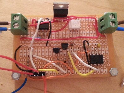
For this project I decided to try out some new prototyping board from Multicomp and as it happens this was identical to what Fritzing called Radio Shack276-150, and is an odd cross between perf-board and strip-board that is aimed at a mix of chips and passive components.
It caught my eye as on the whole I prefer smallish perf-boards these days but having to bridge together the perforations is a bit of a pain.
As a bonus it has marking on the top that indicate where the copper is underneath.
While for this circuit I ended up spreading the circuit over two boards, on the whole I think this size is good for the type of projects I tend to do on prototyping board.
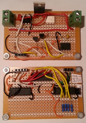
Compared to the Fritzing breadboard layout the big change with the actual hardware was adding 4-way receptacles to act as the interface between the two boards, but otherwise there is little deviation between the two.
Testing
The “upper” board is the high/low voltage interface and the trigger pulse circuits whereas the lower board is the on/off decision circuit, and at time of writing I have not had the opportunity to test them as a single unit. With the phase and enable signal tied together the “upper” board sometimes operates as expected, but without access to an oscilloscope I am unable to determine the root-cause of this unstable circuit behaviour. I will cover proper testing & quantitative evaluation in a future article when I next have access to the appropriate equipment, but at the moment I am unsure when I will be able to do such testing & analysis.List of components
For reference I have included below a list of components used when building the circuit. Some of these are old stock I bought back in 2017 but to my knowledge they were all sourced from Farnell and are still available from them. Use of two different power ratings of 10kΩ resisitors is due to which was closest to hand when building the two boards. At least on the low-voltage side the current draw through all the resistors is well below what a 120mW rating allows but I prefer the physically larger 250mW ones.
| Component | Manufacturer | Part number |
| 72x47mm prototyping board | Multicomp | MC01009 |
| 2-way 12AWG terminal block | MC000034 |
|
| Transistor optocoupler | Vishay | H11AA1 |
| NPN transistor | ON Semiconductor | BC547B |
| Triac-output optocoupler | MOC3021M |
|
| High-current triac | Ween Semiconductors | BT136-600D/DG,127 |
| 555 timer | Texas Instruments | SE555P |
| Logical comparator | CD74HC85 |
|
| 8-bit I/O Expander | PCF8574 |
|
| Digital counter | SN74HC393N |
|
| 0.1μF capacitor | Kemet | C322C104K5R5TA7301 |
| 390Ω resistor | TE Connectivity | CFR25J390R |
| 1kΩ resistor | CFR16J1K0 |
|
| 10kΩ resistor (125mW) | Multicomp | MCRE000049 |
| 10kΩ resistor (250mW) | MF25 10K |
|
| 12kΩ resistor | TE Connectivity | CFR25J12K |
| 78.7kΩ resistor | Vishay | MRS25000C7872FCT00 |