Joule thief
09 October 2021More formally known as a voltage booster this is a circuit I decided to try out as a tangent from my LCD timer, which was an ultra-low current 3.3-volt circuit which by design ran off two 3-volt button cells in series. However even the most forgiving of low-dropout regulators available in
SOT-223 packages are specified for an input voltage north of 4.3 volts — what I was unsure of was where 2.15 volts appears in the discharge curve of a 3-volt CR2032 cell and this eventually lead me to trying out this booster circuit.
In practice I suspect the overheads of boosting the voltage might not be worthwhile in this case and there was no realistic prospect of including one within the LCD timer, but I decided to try building a booster anyway as a mini-project in itself.
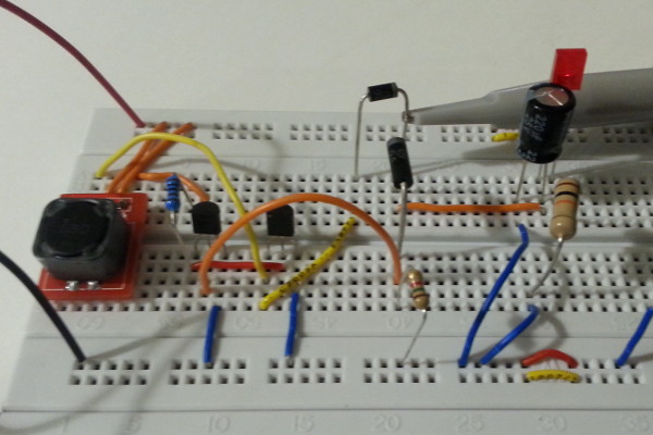
This project was originally intended to only fill in a weekend or two back in September 2020 but since it did not work as expected some further experimentation was planned, and it would be over a year later before I finally got round to finishing off the project. In the process the circuit was completely rebuilt on solderless breadboard using some breakout mini-PCBs and omitting the second-stage voltage regulation.
Circuit design & construction
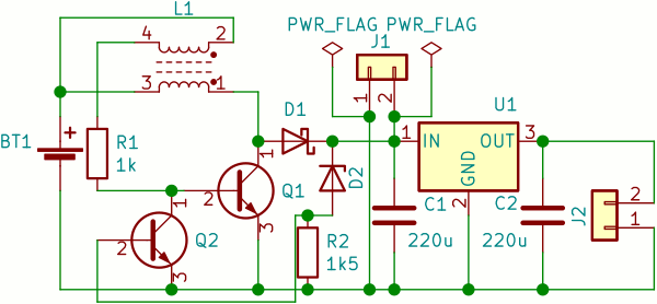
The circuit itself I think originally came from Stackoverflow's electronics section, and I suspect that in turn it was probably copied out of a standard text-book. In the schematic belowL1,R1,Q1,D1 is a basic joule thief magneto circuit whereas R2,D2,Q2
is a feedback curcuit that shuts things down when the output voltage is high enough for the voltage regulator.
Connector J1 is intended as an observation point whereas J2 is the regulated power output.
Fabrication & soldering
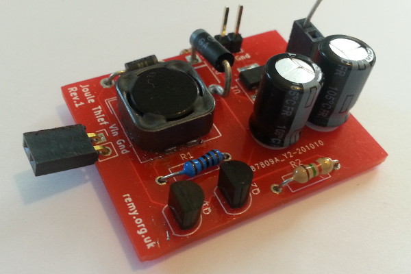
I initially had five PCBs fabricated by JLCPCB as part of the same order as the USB-I2C respin, but since two were damaged during reflow soldering and I felt that the remaining three were insufficent for experimentation with different inductor ratings, I ordered in some inductor breakout boards with the intention of rebuilding the circuit using solderless breadboard. Due to problems with unpredictably long shipping delays I have since stopped using JLCPCB, although that is not a fault of the fabrication service itself. Although I did have a go at both hand-soldering and hot-air reflowing the PCB breakout boards in thre end I resorted to hot-plate reflowing them — the one difference being the use of solder wire added by hand rather than solder paste. I had wanted to use an old stock of Chip QuikSMDLTLFP tin-busmuth solder paste in order to see how it performed when well past its shelf life but never got round to doing so and had to dispose of it as part of my final move back to the UK.
Component list
Below is a list of the components used in building the circuit although although I am not sure if they are the best choices for the task — this list was compiled long ago and the choices were mainly whatever was at hand. The key component is a coupled inductor and all of the suitable ones available from Farnell were surface-mount, which is why I originally opted to design a PCB rather than use prototyping board. I ended up ordering in a small cross-section of inductors with different values from the same series to see what effect inductor rating had on the circuit.
| Item | Description | Manufacturer | Part number |
Q1,Q2 |
NPN transistor | ON Semiconductor | BC547BTF |
L1 |
Dual 47μH coupled inductor | Bourns | SRF1260-470M |
| Dual 68μH coupled inductor | SRF1260-680M |
||
| Dual 100μH coupled inductor | SRF1260-101M |
||
| Dual 820μH coupled inductor | SRF1260-821M |
||
| Dual 1000μH coupled inductor | SRF1260-102M |
||
D1 |
Fast diode | Multicomp | BA157 |
D2 |
4.7-volt Zener diode | ON Semiconductor | 1N5337BRLG |
C1,C2 |
220μF capacitor | Panasonic | EEU-FR1E221 |
R1 |
1kΩ resistor | Multicomp | MF25 1K |
R2 |
1k5Ω resistor | MCF 0.25W 1K5 |
|
U1 |
3.3v low drop-out regulator | Diodes Inc. | AZ1117CH2-3.3TRG1 |
Experimentation
I initially used a 100μH inductor but it soon became apparent that it was only boosting the voltage up to around 3.5 volts rather than the circa 5 volts so I ordered in other inductors of different ratings to see what effect they had on the output. However in practice this made no difference to the smoothed output. The oscillopscope trace below was taken with the capacitor removed; green is with an inductor value of 47μH, yellow is 100μH, and aqua is 1000μH — note that the three traces are not to the same time-base scale.
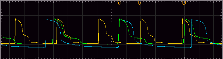
The peak voltage of 5.6v is roughly the sum of the expected zener voltage plus the base-emitter voltage drop so the problem is the duty cycle of roughly 10-20% only being able to bring the smoothing capacitor up to a touch under 3.6 volts, and on the original PCB this was insufficent input to the voltage regulator. Realistically the only fix is to use a zener doide with a higher reverse-voltage