MOSFET transistors
06 February 2021Back in 2017 when I had barely got started with electronics I looked at BJTs (Bipolar Junction Transistor) and mostly used them as simple switches but more recently I have been using them to manually build logic gates, and decided to have a look at MOSFETs (Metal-Oxide-Silicom Fields Effect Transistors) to see if they would be suitable for the latter use-case. This article is my personal notes from the reading up I did trying to trying to understand them.
Types and modes
There are two modes of operation for MOSFETs, depletion and enhancement, the difference between the two modes being whether the transistor is on or off when the gate voltage is zero. Within each mode there are P-types and N-types and the symbols for all four combinations are shown below. The broken vertical line indicates an enhancement mode MOSFET whereas depletion mode MOSFETs this line is continuous rather than in three pieces; the arrow points in for N-type and out for P-type. This article will only consider the enhancement mode variants.
| Type & Mode | Symbol (standard) | Symbol (simplified) |
| P-type enhancement mode |
 |
 |
| N-type enhancement mode |
 |
 |
| P-type depletion mode |
 |
|
| N-type depletion mode |
 |
|
MOSFET part numbers
After some digging I settled on the following descrete MOSFETs which I selected due to them being available individually in aTO-92 style case, which is the “traditional” transistor case.
At around 35-40¢ each when bought in bulk they are very expensive compared to BJTs, which I am guessing is due to their relative lack of popularity for through-hole circuits.
My general impression is that for purposes requiring depletion mode FET transistors, JFETs (Junction FETs) would be a cheaper alternative but they are beyond the scope of this write-up.
| Description | Manufacturer | Part number | Order code |
| P-Channel Power MOSFET | Microchip | TP2104N3-G |
2775067 |
| N-Channel Power MOSFET | TN5325N3-G |
3580722 |
CMOS circuits
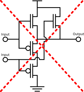
The P-type is effectively active-low and the N-type active-high, so there is a simplification where the P-type is shown with a negation bubble on the input, and it is assumed that the source pin is always orientated towards the power rail — Vcc on the P-type and ground on the N-type. The idea behind CMOS (Complimentary MOSFET) is that P-type and N-types between them always pull the output high or low, which is easily seen with the CMOS Not-Gate shown below.

It need not be a one-to-one pairing — in the NAND-Gate below the output is pulled low when both inputs are high, but if either input is low then the output is pulled high. Obviously the logic of the high and low side should be such that the output is not pulled high and low at the same time.

A nice thing about CMOS circuitry is that since the MOSFETs are high-impedence inputs there is no need for any resistors. In practice P-types are always on the high side and N-types on the low side, since swapping them around screws up their electrical properties in ways that don't ensure fast switching. This is why an And-Gate is usually implemented by taking a NAND-Gate and putting a Not-Gate on the output, rather than swapping P-types for N-types and vice-versa.