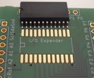
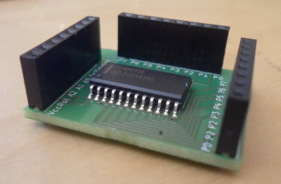
PCA9671 breakout
03 February 2018This article is a follow-on from my TCA9535 expander breakout, this time using an NXP
PCA9671D 16-bit I/O Expander (Farnell 2212104), which is significantly larger SOIC chips compared to the SSOP chip used in the previous breakout board. It is also a practical excercise in using KiCad for the first time to design a PCB rather than Fritzing, so a large portion of this article will cover the building of the breakout board.
This expander is operationally pretty much a 16-bit version of the Texas Instruments PCF8574 in that it is an open-drain expander that does not have any configuration state. It can use one of 64 different addresses, and according to the data-sheet it can have all 16 of the I/O pins drawing 25mA each (400mA total) which is a lot.
PCB design using KiCad
For this PCB I decided to give KiCad a try-out, as I found Fritzing to be seriously lacking when it came to SMD components, and there was no way I was going to touch any “free” programs that are subscription-based cripple-ware. KiCad clearly shows a lot of its 1990's MS-DOS heritage, but once you start to work out all its resulting idiosyncracies which are in part due to its power, it is actually quite nice to use. The one difficulty is that it was obviously originally designed as seperate programs that follow the waterfall model, so going back to the schematic to make changes is not quite straight-forward.Schematic layout
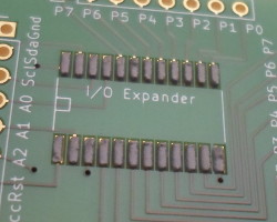
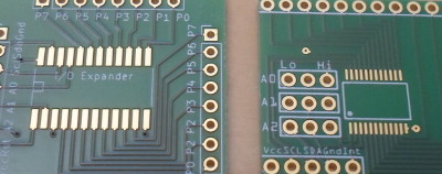
The schematic for a breakout board is not particularly complex, but I include it here for completeness. ThePCA9671D schematic component is one I made myself, but this is actually quite easy to do once you get the hang of it, and in fact creation of such components is something one seems to be expected to do. Here it is simply wired up to three generic 8-way connector components.
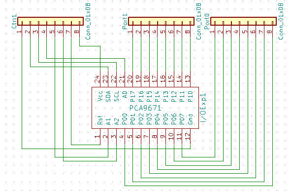
Note that this is a 1:1 screenshot from KiCad's eeschema, so the scaling artefacts are seen in the program itself rather than being the result of subsequent image processing.
PCB layout
In KiCad schematic components and PCB components (termed footprints) are independent entities, unlike with Fritzing where each component has a selection of possible PCB forms. When moving from schematic design to PCB design KiCad requires the choosing of a PCB footprint for each schematic component, the only limitation I am aware of being a matching number of pins. For instance in the schematic above the connectors are “generic&rd180; 8-way connectors, but on the PCB I could for choose either 8-way pin headers or 8-way receptacles. Below is the completed PCB view for the breakout board:
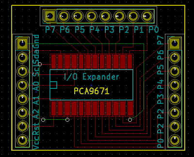
For this board I had started out making my own footprint from scratch, but ended up using the stock SOIC-24 footprint from the SMD_Packages library instead. However at the last moment I had doubts about whether this stock footprint had the correct dimensions so I extended the pads out an extra millimetre, which turned out to be a good move as my doubts were correct, although in hindsight I should have instead moved the pads 1.5mm — 1mm extra was only just enough, and the pads extended under the chip itself rather than just the pins.
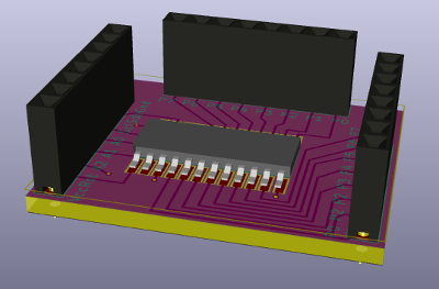
3D PCB view
KiCad includes a 3D view which by any measure is a nice feature, although I am not sure how essential it actually is, and it was one of my motivations for using a stock footprint rather than making my own from scratch. Whatever its usefulness, I do feel it gives an accurate presentation of what the final board will look like:
Overall view of KiCad
KiCad started life in the early 1990s, and it is clearly still influenced by its MS-DOS heritage. Rather than a single program is it really a collection of programs that are not exactly consistent in how they present things, and there is the heavy use of hotkeys rather than mouse clicks even for basic things such as moving components around. It is quite nice once you get the hang of it, but it results in quite a steep learning curve which is quite irritating at first. There are moves to improve the user interface, but I doubt it will truly be integrated anytime soon. Fritzing is quite forgiving about going between schematic and PCB views, but KiCad is a lot more waterfall-orientated, and at the time I was designing this board I did not know how to change the schematic without screwing up the PCB.Doing the reflow
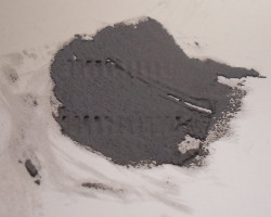
This is far from the first time I have done reflow soldering, but it is probably the first time that everything has gone exactly to plan. No solder bridges so no need to do any rework, and the whole process went smoothly. The three picture below summarise the placing of the solder paste, a particularly notable thing being how little is actually needed.
The reflow itself I did on the hot-plate, with the molton stage happening after 6-8 minutes when the chip temperature got to some point above 140°C — I stopped checking with the infared thermometer and started a recording the melting around this point, so did not find out the melting point.
Solder paste
Although I do have a stock of what should be high-quality Tin-Bismuth solder paste, so far I have been using up a stock of cheap Tin-Lead solder paste that gets the job done but is a pain to handle. The latter came in a syringe but it is far too viscous to try to apply with any real precision, either direct from the syringe or using cocktail sticks, so scraping it over a solder mask is the only practical way of using it. Quite likely it is supposed to be stored in a tub and stirred well before use, and possibly the granual size was an issue with SSOP-sized components. I got this cheap solder paste because I was (incorrectly) assuming that my first attempts at reflow soldering would go wrong, but once I use it up and start using the Tin-Bismuth stock I suspect I will look back and wonder why I put up with the former.Solder Stencil
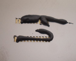
For the TCA9535 breakout I decided to do without a solder stencil, which in hindsight was a major mistake. Stencils are not exactly cheap for what they are, but this time round I decided to bit the bullet and order one with the breakout PCBs. They make the process of putting down the solder paste so much quicker and easier, particularly as I now know how to do it in such a way that minimises mess.Expander operation
Much like thePCF8574, the PCA9671D is a zero-configuration expander with open-drain outputs that either sink current or are high-impedence; when in the latter state the pins are driven by the external circuit and can be read — there is no actual setting of pins as input or output. The expander does not use internal addressing (i.e. it does not have addressable registers) so an I2C master simply issues a read or write depending on whether it wants to poll or drive a pin. Below demonstrates using the expander.
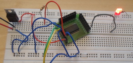
USB-ISS setup
For demonstration purposes I will use my usual Python TxRx script coupled with the USB-ISS adapter. Before using it, it needs to be set to I2C mode using the following command-line. Rather than0x60 which selects 100kHz as the I2C clock-rate, 400kHz can be selected using 0x70, and 1MHz using 0x80, if so desired:
./ttyTxRx.py /dev/ttyACM0 2 5a 02 60
Device addressing
As well as Vcc and Ground the three address pins of thePCA9671D can also be connected to the I2C clock and data lines, which expands the number of possible I2C addresses to 64. The addresses that just use Vcc & Ground are the same as the TCA9535, and the entire mapping is in a Table 3 (pages 6 thru 8) of the data-sheet. The address mapping from what I can tell is standardised across at least all expanders I have experimented with.
Device reset
I don't know why thePCA9671D includes device reset, done by either pulling the reset pin low, or issuing a I2C GCA (General Call Address) transaction, because the device has practically nothing in terms of configuration state to reset. All it does is to set all input pins to high (i.e. open-circuit, off basically). Doing a reset using the GCA involves writing 0x00 followed by 0x06, which the following command-line will do:
./ttyTxRx.py /dev/ttyACM0 1 53 0 6
Device query
I am not sure why this query is available, but I have the suspicion it might be a standard query shared by multiple vendors. It returns 3 bytes that state codes for the manufacturer, part number, and part revision. It requires a custum I2C transactions that is constructed as follows:
| Custom I2C | Start | Write 2 bytes | Restart | Write 1 byte | Read 2 bytes | Schedule Nack | Read 1 byte | Stop | |||
| 0x57 | 0x01 | 0x31 | 0xf8 | addr | 0x02 | 0x30 | 0xf9 | 0x21 | 0x04 | 0x20 | 0x03 |
This transaction can be dispatched using the command-line below, which also includes expected output. The first two replies are status from the USB-I2C adapter, with 0x0002a0 being the query response.
./ttyTxRx.py /dev/ttyACM0 5 57 1 31 f8 be 2 30 f9 21 4 20 3 Sending 12 bytes.. Sent 12 Replies (5 expected): 0xff 0x3 0x0 0x2 0xa0
Writing
Writing pins is a simple writing of two bytes, corresponding to the two ports, which can be done using the command-line below. When a pin is set high it is “off” and when it is set low it acts as a current sink. The following would set all of Port 0 high and all of port 1 low:./ttyTxRx.py /dev/ttyACM0 1 54 40 2 ff 0
Reading
For pins that have been set low by a write a read will return low, but for pins set high the return value is whatever the external circuit is driving the pin to be. Reading pins is just a case of issuing an I2C read transaction to obtain the values of the two ports, which can be done using the command-line below../ttyTxRx.py /dev/ttyACM0 2 54 41
The only complication is that pins that are intended to be read should be set high by any previous writes, otherwise the open-drain output will mask whatever state the external circuit is trying to drive.
Integrated circuit size
One reason for choosing this expander was to see how the larger chip size compares with the much smallerTCA9535, in particular the much wider spacing between the pins. The latter has extensive bridging even after trying to put what I thought was minimal amounts of solder paste onto the pads, but even this proved too hard to do by land. The image below gives an indication of the relative sizes:
A while ago I ordered in three sizes of the same SMD resistor to see how the sizes compared, and as a result decided that I would avoid getting resistors & capacitors smaller than 0603 (1608 metric) and that I would aim for 0805 (2012 metric) or larger, as the increased difficulty of components I could barely see is not worth the real-estate saving. Unless absolutely necessary I an inclined to avoid components that need a microscope to place accurately.
Remarks
I put in the effort for KiCad because I was informed it was up there with Eagle in terms of what it can do, and having used it end-to-end I feel that any return to Fritzing will be steps backward. I generally expect future PCBs I design to include SMD components, which is where Fritzing starts to show its shortcomings. KiCad's parts & footprint libraries have their own set of issues, but at least it is not that much of an issues to modify stock parts. I have found the register-based nature of theMCP23017 and the TCA9535 to be complexity without worthwhile benefit, so for the PCA9671D to take the zero-configuration approach of the PCF8574 is a favourable thing from my perspective. It is a pity that there is not through-hole version of this I/O expander, because if there was I would have used it for my LED matrix row driver and my 7-segment LED.
My motive for trying out SOIC chips was due to the looser tolerances compared to SSOP chips. The main one was my own visual tolerance, as all the SMD components I had used previously I was able to place without any magnification, but for placing an SSOP chip it was a different story. I suspected the small size was causing problems elsewhere — even with a stencil mask the probable quality of solder paste may still have caused problems due to it being course-grained and viscous, making it harder to place and more prone to solder-bridging on smaller pins. I also suspect the larger chip sizes also allow bigger current draws. On a similar note I decided that resistors and capacitors smaller than 0603 (1608 metric) should be avoided, as that size I feel that size is the smallest that is reasonably forgiving.