Hard-wired digital de-bouncing
30 May 2022This circuit is an entirely hard-wired digital button-press debouncer that makes use of logic chips rather than a micro-controller running firmware. Although not an economic way of implementing such functionality compared to doing the task in firmware it is a project done for the process rather than the outcome. This circuit is intended as a return to doing electronics now that all my components and equipment are in one place following my return to the UK, and it is one of many that were designed during the dark days of Covid-19 lockdown but got delayed in their implementation and write-up. I am not entirely sure when I conceived the idea of using only logic chips rather than using firmware for debouncing as I had made other “hard-wired” circuits in late-2020 and early-2021 but the only hard evidence I could find of working on a debouncer design pointed to April 2021.
Debouncing circuit design
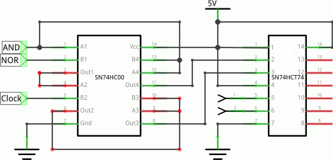
This debouncing circuit is a hard-wired version of the PIC16F630 debouncer and an overview is shown in the schematic below. The basic idea is to sample the input at regular intervals, and if all the eight most recent sample bits have the same value this value becomes the output; when there is a mix of high and low samples, it is assumed this is due to transient instability and the previous value is maintained as output until all the samples have become the same. The circuit splits up into three parts — a sampling sub-system, filtering logic, and output latching — which are all indicated on the schametic
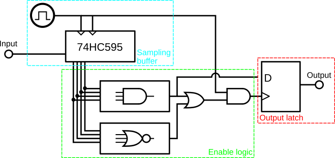
Sample clocking
The clocking of the whole circuit is provided by an astable 555 timer chip, the setup of which is summerised in the schematic below; the choice of component values for the capacitor and resisitors was a play-off between what clock period was desirable and what components were in stock, which in practice worked out well. If the 10kΩ potentiometer is set to its mid-point of 5kΩ the calculated clock period is 0.2mS which means eight samples covers 1.6mS which from previous experiments is long enough to outlast typical bouncing transcients. This is notably different from the sample window calculated for the firmware-implemented circuit but I suspect the calculations done at the time for the latter are inaccurate.

Sampling buffer
A74HC595 shift register is used as the sampling buffer, with a new sample shifted in from the button on each clock cycle and at the same time the oldest sample residing in the most significant bit latch gets discarded, so the eight parallel outputs represent a sampling of the input over 1.6mS and this output is is used as input to the next stage.
The parallel output from the shift register is one clock cycle behind what is in the internal buffer so the debounce logic does not actually have the absolute latest sample;
this is a property the shift register has in order to avoid race conditions when the data clock and buffer-to-tristate transfer signals are tied together.
The resulting lag is not critical in this application, although inverting the transfer signal so it occurs on the falling edge was considered as a work-around.
Enable logic
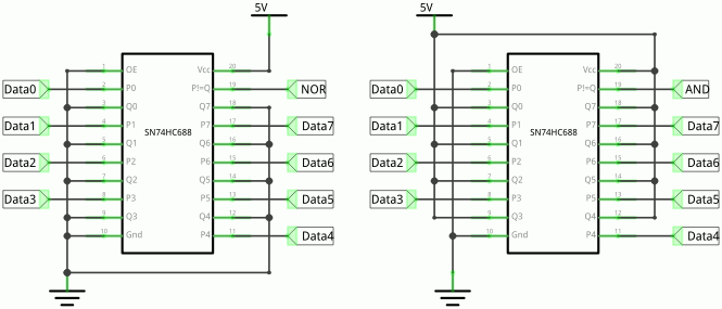
The overall aim of the enable logic is to indicate when the samples within the shift register are either all high or all low, and these two cases are individually detected then OR-d together to produce an update-enable signal. Although presented in the schematic as multi-way AND & NOR gates, these are implemented using74HC688 identity comparator chips that compare the shift register output with an all-high and all-low reference respectively, and the wiring of these is shown in the schematics below.
The outputs of these two comparators — labelled AND and NOR respectively — is then combined which since the output of the comparators is active-low is done using a NAND gate to provide an active-high OR output.
A single quad 2-input NAND gate chip is used to get all the signals for the output stage, and a schematic for its wiring as well as that of the output latch is shown below. As far as I am aware this is the simplest way to implement the enable logic sub-system using hard-wired components — it could be reduced to a single chip by using a logic array or an EEPROM but these are self-defeating solutions given that the whole purpose of this project is to avoid programmable chips.
De-bounced output
When the enable logic indicates that all the sample bits are the same it provides a signal that indicates this value as well as un-gating a clock so that the value is latched using a74HCT74 D-type flip-flop, which then maintains this value when the bouncing input subsequently reenters a transient state.
The output of this stage is the final debounced output for the entire circuit.
Building the circuit
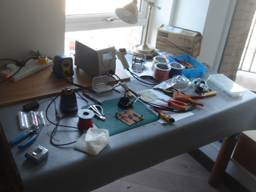
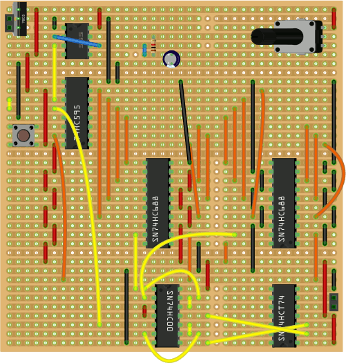
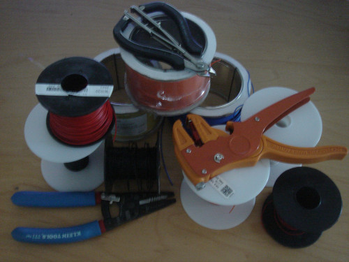
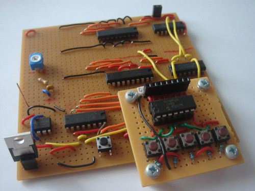
I have tried all sorts of exotic prototyping boards but I have found a lot of them are better in theory than in practice. For instance I had high hopes for Busboard which is a variant of perf-board where holes are paired in order to avoid the need to wrap wires around the legs of components, but it had the pairs orientated parallel to the long edge rather than the short edge and it only really works when any given component leg is connected to only one other — otherwise it is back to bridging hole together as with classic one-hole perf-board. By the time I was thinking of perf-board with holes grouped into threes or more I am basically back to strip-board that in effect allows the hole groupings to be customised. For a project like this which mainly uses integrated circuit chips the MulticompMC01010 would be a natural choice but I doubted it was big enough for the number of chips this project requires, and I have stopped looking for any alternatives as ones I find are invariably overpriced.
So strip-board it is for this circuit.
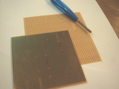
Cutting the tracks
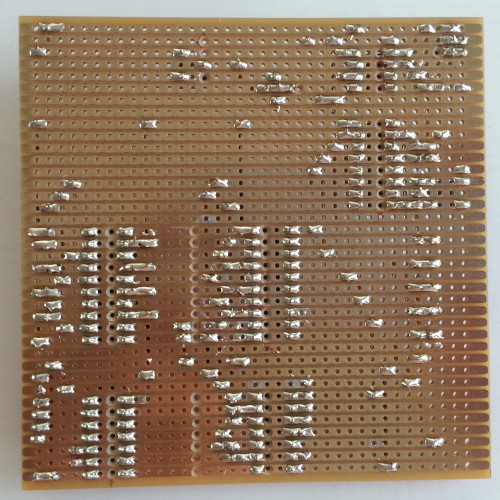
When using strip-board the need to cut tracks means laying out the circuit in a circuit design program first and to date the only one I have found any good for prototyping board is Fritzing — yes it has its issues but the other circuit layout tools out there that are any good target PCBs instead, and after a few years I have got used to many of Fritzing's idiosyncracies and working around its outright bugs. Once laid out a flipped screens-shot of the board with all components removed is a handy guide for cutting the tracks, and having a to-scale printout helps avoid mistakes when counting the holes between cuts.
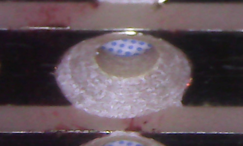
Of course due to the way Fritzing presents tracks an export of the circuit with all components removed needs to be flipped since the tracks are cut from the underside. When all the cuts have been done they then need to be checked with a multi-meter to make sure electrical contact has indeed been broken as it is all to easy for a small slither of track to remain as shown in the microscope picture below. Hard to see without magnification but it is enough to screw up the circuit, and with this circuit there were about a dozen holes needing further drilling to ensure no connection remains.
Sourcing the components
I have lost track of when many of them were sourced but this project intentionally made use of components I already had in stock and where known they are listed in the table below with manufacturer names and part numbers. Vendor order codes have been omitted because for some of the items I have lost track of which vendor was used to source them, and in more recent months I have noticed a sharp increase in the number of components that are out of stock with long lead times or have been discontinued. In addition some manufacturer names have changed since certain items were obtained.
| Component | Manufacturer | Part number |
| Tactile button | TE Connectivity | FSM4JH |
| 5-volt TO-220 regulator | Texas Instruments | UA7805CKCS |
| 555 Timer | NE555P |
|
| Serial-to-parallel shift register | SN74HC595 |
|
| Identity comparator | SN74HC688 |
|
| D-Type latch | SN74HCT74 |
|
| Quad two-input NAND gates | SN74HC00 |
|
| 10kΩ trimming potentiometer | Amphenol | N6L50T0C-103-3030 |
| 4.3kΩ Resistor | TE Connectivity | CFR25J4K3 |
| 22nF Capacitor | Vishay | K223K15X7RF53L2 |
| 2-way receptacle | Multicomp | 2212S-02SG-85 |
| 10x10cm strip-board | Kemo Electronic | E012 |
| 183°C Solder | Edsyn | SS5250 |
| Red hookup wire | Unknown | |
| Yellow hookup wire | Concordia Technologies | EW1/0.6TYELL100M |
| Orange hookup wire | EW1/0.6ORG100M |
|
Using good wire
Even to this day the best wire I have ever used is a reel of unplated solid copper I got from Maplin back in 2017 and I have since then with mixed success tried to source something comparable — the nearest I have found I am pretty certain has the same wire thickness but is plated copper and I am unsure of the wire coating. Plated copper does not seem to wick up molton solder quite as well as pure copper and I also had issues with some wires I got in not being strong enough to avoid breaking when being stripped. For this project the combination of Concordia Technologies PVC coated 23 AWG wire and a Duratool808-080-F wire stripper has worked well, although the slower to use Klein Tools 11057 is better matched to a range of wire guages.
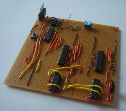
The completed circuit
The actual construction of the circuit — in other words cutting of the tracks and soldering everything in place — was a stop-start process that in itself took just under two months end-to-end although much of the actual effort was concentrated in two or three sittings. There were plenty of mistakes such as wires going to the wrong tracks that thankfully I spotted but such mishaps is perhaps to be expected given how long it has been since I did anything this complex.
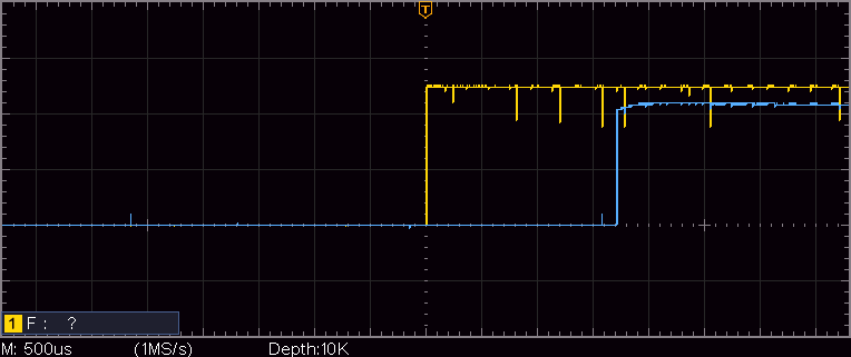
A basic test was to trigger on the rising edge of the button and attach the second oscilloscope probe to the output and the resulting traces were as expected, and this is reproduced below. There is clearly noise on the power tracks but a bypass capacitor across the power tracks would sort this out. Otherwise the circuit operated as intended, with the delay between button press and the output going high being around the 1.6mS of the sampling window although it did vary a bit as would be expected with some bouncing.
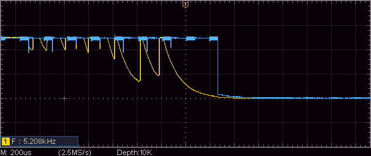
In practice bouncing is more a problem with button releases than button presses, as can be seen in the trace below which shows the most dramatic release bouncing I was able to obtain from some quick testing. In this case I suspect that the sampling actually missed some of the up-spikes because the output went low a lot earlier than I would have otherwise expected it to do so but nevertheless the debouncing was still successful. The circuit may indeed actually have faults but the results here show that the general architecture is sound and operating as designed.
Remarks
This project highlights the flexibility of microcontrollers and by any measure there is no practical sense in implementing debouncing digitally using hard-wired components as has been done here — this circuit needs six chips to do what my previous firmware-implemented debouncer needed just one chip for, and even then the latter has five buttons as opposed to the single one on this cirucit. These days a large portion of digital processing circuits are pretty much just support infrastructure for a microcontroller chip and all the actual algorithmic stuff is written in firmware. However I design and build electronic circuits because I want to do something other than write program code, hence why I conceived this project in the first place; needless to say I wanted to spend my time soldering rather than programming.
The project started as a lockdown-era project which I suspect was first conceived early April 2021 and its final completion marks a proper return to doing electronics as a hobby, and as a result is a personal mile-stone in getting on with my life. Like many other project done in the last 18 months it has been very start-stop so unlike earlier projects I am unsure exactly when work was done on it — in fact last year I built up a back-log of completed circuits so that I had stuff to write about while back overseas. I have another project in the design phase at the moment but I am unsure how quickly I will complete it.