Programming the MKE02Z64 Cortex-M0+
10 November 2019When the 2nd generation LCD dot-matrix display was made I decided that I would cover the ARM Cortex-M0+ firmware in a seperate article, covering details in a generic way due to the amount of expected overlap with the LED dot-matrix controller. These circuits used Cortex-M0+ chips rather than PIC microcontroller I typically used previously, because they involve the type of data-processing that PIC chips are very poor choices for.
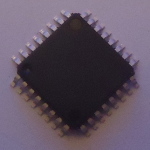
Although made by NXP the Cortex-M0+ chip used is one NXP inherited when they took over Freescale semiconductors in 2015, so the chip does not follow the usual NXP conventions. The chip is part of the Kinetis E family of ARM Cortex-M0+ based microcontrollers, and within this family it is within the KE02 sub-family. I am unsure of the level of compatibility with the KE04 sub-family but at a glance the only difference seems to be the number of pins. From the data-sheet the part number splits up as follows:-
M |
KE02 |
Z |
64 |
V |
LC |
2 |
| “Qualification” | Subfamily | Core (Z=M0+) | Flash size (in kB) | Temperature (-40 to 105°C) | Packaging | Max CPU speed (20Mhz) |
Some of the parameters such as qualification are clearly superfluous, since the publicly available parts only have one available value. The documentation uses KE02Z as the family code, although I think it is more correct to use MKE02Z64 when referring to the chip in a package-independent way.
Using the microcontroller chip
In common with other ARM-based chips I have used, firmware is written with in C using the ARM GCC tool-chain, so once the linker scripts are sorted out it is not much different from the low-level Linux development I have done for the last two decades. Attaching a debugger is a little more involved, and there are limitations such as the number of break-points available, but otherwise there is no operational difference. The following sub-sections cover GPIO and serial communications functionality.Using general-purpose I/O
An odd thing with the Kinetis series is that it has two separate interfaces for GPIO access, which aside from different base addresses are identical — they seem to use different hardware paths and I have seen hints that some other related chipsets don't have one of them. I opted to use the FGPIO interface which is the one located at0xf8000000. In contrast to the LPC10xx series which uses masks for setting/clearing pin values, the Kinetis instead uses set & clear registers — which while less flexible is a better approach in cases such as this circuit where bits are set or cleared individually rather than in parallel. The lcdSetup() function of the LCD display firmware shows everything needed to setup and toggle GPIO pins, and this function is partially reproduced below:-
REG(0xf8000014) = 0x030fff00; // Port mask REG(0xf8000008) = 0x030fff00; // Clear bits REG(0xf8000004) = LCD_CS2 | LCD_RESET; // Set bits REG(0xf8000004) = 0x3f << 8; // Set bits /* delay omitted */ REG(0xf8000008) = LCD_CS2; // Clear bit REG(0xf8000004) = LCD_CS1; // Set bit /* delay ommited */
All but four of the GPIO-capable pins default to GPIO and of the four that don't three of them are used for programming/debugging functionality. All the essential information for FGPIO within the reference manual is contained within four pages (581–584), so there is not really that much to know in order to get up-and-running. This makes a nice change from PIC chips that tend to have analog functionality as reset defaults. However pin functionality is selected by whether various sub-systems are active or not, and they are subject to a priority ranking, rather than each pin having dedicated mode bits within a register.
Configuring internal chip clocking
TheMKE02Z64 uses a 32.25–39.0625kHz (nominal 32kHz) RC timer that feeds into a FLL and the output — ICSFLLCLK within the user manual — is 16–20MHz. This is then fed into frequency divider BDIV controlled via 0x40064001 which has seven possible scaling values between 1:1 and 1:128 and of these 1:2 is listed as the default. The output of the latter is used as the main clock, and various hints in the data-sheet suggest it is a nominal 8MHz. There is a second down-stream divider BUSDIV controlled via 0x40048018 that only affects the bus and flash clocks, but even though it has a dedicated 32-bit register it only supports two scaling choices: the default of none, and divide by two.
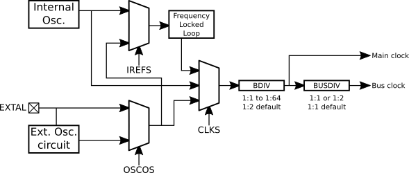
Using a multi-meter to measure the actual frequency of a simple timing firmware toggling a GPIO pin at a 50% duty cycle with a period of 16,000 tics showed a reading of 994.6Hz, indicating an actual bus frequency of 15.91MHz. Checking the BDIV and BUSDIV registers using a debugger showed them to be the default values stated in the documentation, and changing BDIV resulted in the expected relative change in toggling frequency based on stated frequency divisions.
From all of this the simplest conclusion is that the nominal output of the FLL is actually 32MHz. Having to figure this out experimentally leaves me unimpressed, and for tasks that need a known & accurate clock frequency I would recommend use of an external reference.
Using the Periodic Interrupt Timer
With the original LCD-based timer which used aPIC16F1828 clocked at 4MHz, the time it takes to execute a single No-Op is a long enough time delta for pulsing the LCD display's signal pins, but on the 2nd-generation circuit with the Cortex-M0+ clocked at much higher speeds there is the requirement for timed waits.
For this I used the PIT (Periodic Interrupt Timer), and the code fragment below is a minimalist loop:
REG(0x4004800c) |= 0x02; // Activate timer clocking REG_PIT_MCR = 0; while(1) { REG_PIT_LDVAL0 = 16000000lu; REG_PIT_TFLG0 = 1; REG_PIT_TCTRL0 = 0x01; while(REG_PIT_TFLG0 == 0) { } REG_PIT_TCTRL0 = 0; /* ... */ }
In practice the timer would be either be polled in a much larger event loop, or interrupts would be used instead of polling. For most of the microcontroller firmwares I have written so far I have tended to avoid interrupts as they needlessly complicate program flow.
Using the Real-Time Clock
In addition to the periodic timer there is also the RTC (Real-Time Clock) that can operate in much the same way but also has access to other internal clock sources and has binary-division as well as power-of-two frequency division. However I decided not to try it out myself, because issues with the main clock make me disinclined to believe its actual accuracy compared to the periodic timer.Using the RS232 UART Having a UART that supports RS232 is basically a must-have for microcontrollers, and although somewhat archaic from the perspective of personal computers having been de-facto phased out sometime in the early-2000s, it is a well-understood protocol that in most cases gets the job done. A lot of USB devices are really just RS232 devices with an on-board USB-RS232 conversion chip, a simplification I used myself with my USB-I2C adapter. The code below — which echoes all received data — shows everything that is needed to use RS232:
REG(0x4004800c) |= 1 << 21; // Enable UART1 clock REG8(0x4006b000) = 0; REG8(0x4006b001) = 104; // 9600 BAUD REG8(0x4006b002) = 0; // 1 stop bit; no parity REG8(0x4006b003) = 0x0c; // Enable both Tx and Rx while(1) { while( (REG8(0x4006b004) & 0x20) == 0 ) { // Wait for Rx to have data } data = REG8(0x4006b007); while( (REG8(0x4006b004) & 0x80) == 0 ) { // Wait for Tx to become idle } REG8(0x4006b007) = data; }
The UART has a sampling rate that is 16 times the target BAUD rate, and the reference manual presents some calculations for what difference in BAUD can be tolerated before errors get flagged up — for the typical eight data bits, parity, and one stop bit this is 3-4%.
I wrote a Python script that works out the best parameters for a target BAUD given a main clock frequency and BDIV divisor.
If a BAUD higher than 9,600 is required I would recommend using an external clock source, as I have read hints that the accuracy of the internal nominal-32kHz oscillator is not really up to the task, and I suspect that the use of a frequency-locked loop rather than a higher-frequency reference is particularly vulnerable to glitches.
Compared to the LPC11(U)xx where RS232 BAUD is specified as a fraction using multiple registers, setting the rate on the MKE02Z64 is rather primitive in that it is purely integer sub-division of the main clock. To make matters worse the granularity of the divisor is limited to multiples of 16, so some values cannot be obtained without either adjusting upstream clock prescalers that also affect other parts of the chip, or changing the trim of the main reference oscillator. On the plus side an interesting feature I saw in passing was the ability to chain together the UART and the FTM (FlexTimer Module), which is intended for RS232 over infra-red links, but for the time being I have no plans to try this feature out.
Using I2C functionality
Making use of I2C functionality on the Kinetis is pretty much a direct implementation of the flow-chart in Figure 30-30 (Page 544) of the user manual, which is a lot easier than figuring out I2C on the Microchip PIC microcontrollers. Although multi-master and simultaneous master & slave setup are supported, I am only really interested in two simpler setups: Single dedicated master and single dedicated slave — these are detailed below. I opted to use the defaultPTA2 & PTA3 pins for I2C since they are true open-drain pins, although PTB6 & PTB7 can also be used by adjusting bit five of register 0x40048008 (user manual pages 156–157).
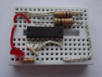
To test I2C master firmware I wired up a PCF8562 expander as shown below. The one tricky bit is choosing the value for the I2C BAUD rate register, for which I wrote I wrote a Python script.
Most of the actual trouble I had getting slave mode working was down to incorrect use of the Robot Electronics I2C-USB device rather than problems with my firmware, although a minor gotcha is that registers are cleared by writing a 1 rather than masking out the relevant bits using an AND operation. How to use I2C slave mode is shown in a serial demo firmware where I2C status is written to the RS232 connection and I2C reads use incrementing byte values.
Review
A lot of the concepts I already knew from previous Microchip PIC programming, and on the whole this is a chip I now quite like to write firmware for now that I have worked it out. However the process was a lot more of a headache than it should have been, and it is the only chip I have ever bricked via firmware — I have damaged other chips in the past, but this was either physical damage, or chips that were of questionable quality to begin with.Clock accuracy
I had to resort to experimentation to find out the actual frequency of the chip, and the values I ended up with were not in line with what I had expected from reading the user manual. There is an additional on-board 1kHz clock but for some strange reason is only available for the watchdog and real-time clock and cannot be used as the main clock, and in any case after trouble with the main clock I am reluctant to trust the specifications for any of the internal clock sources. In short the internal clocking seems patently unsuitable for any tasks where a known and accurate operating frequency is required, and one of my future plans is to try using an external crystal or oscillator. The MulticompMCSJK-6NC1-16.00-25-B (Farnell 2854365) is of particular interest since it is self-contained.
Quality of the documentation
The Kinetis E series data-sheets and user manual are noticeably different from NXP's usual style, due to the chip being designed and produced by Freescale Semiconductor before it was subsumed into NXP. There seems to be an assumption of prior experience with other ATM chips, as things like general ARM Cortex-M+ information tend to be omitted, whereas the documentation for theLPC11(U)xx families is much more self-contained. While the Kinetis documetation generally contained the information I needed, I felt that it was nevertheless of poorer visual quality than NXP's own style, and in places I wondered whether it had actually been proof-read end-to-end.
A major irritation however is information on clocking — the LPC11xx series is straight up with the reset-default clock speed being 12 MHz, but with the MKE02Z64 I took a guess that it is a nominal 16MHz, although basic experimentation suggested otherwise.
Compared to the documentation of other NXP components I have used in the past, the Kinetis documentation is disappointing. It does have some very good sections that are down to the point, but large parts of the documentation feel like they were originally written to be stand-alone, as if they were mini-datasheets for sub-systems that were simply cut'n'pasted into the manual for the chips that use them. At quite an early stage I concluded that, due to what the documentation omitted — even though I figured out it was typically general ARM stuff rather than chip-specific — I simply cannot recommend this chip to anyone who has not had previous ARM experience with another product.
Comparison to Microchip PIC programming
A fundamental issue with Microchip PIC firmware programming is it really has to be done using assembly rather than C, as the instruction set is unsuited for targeting by a compiler. I never tried Microchip's own development environment, which ought to do a better job than the open-source SDCC, but it is not going to be able to get away from limitations such as not having local variables. The PIC assembly set does have some nice features and in particular it allows for tight programming with predictable execution times, which in turn allows for close matching of clock speed and timing tolerances. However the PIC architecture is very much geared towards highly procedural pin control which requires very little state, and is rather painful to use when the main task of the microcontroller is handling of data — the instructions are very good for handling individual bits, but the banked memory model gets very painful when storage requirements are more than a few dozen mostly-independent bytes.While a part of me does miss PIC assembly there are relatively few projects I actually used it for the firmware in preference to C and in most cases I would be better off using ARM — C is the level of abstraction I normally think at, most of the time I just want to get the firmware done, and for C the development eco-system is simply a lot better. In practice PIC's notional advantages don't translate into lower costs. In addition, whereas I think it is very unlikely that I would ever use PIC microcontrollers professionally, having to do this type of bare-metal programming of ARM chips is within the bounds of realistic probability — at time of writing my professional work involves getting my fingers dirty with UBoot on an ARM-based Linux platform, and a professional future with ARM is why I started looking at Cortex-M chips in the first place.