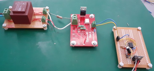
Opto-coupled triac PCB
03 September 2024This is a long-overdue PCB version of the high-voltage interface used in the AC power phase-control circuits I built back in 2020 and 2021, the sole purpose being to have the mains power switching part of any circuit well separated from the rest for safety reasons. Having this self-contained and dedicated circuit is due to having in the past getting electric shocks even though I was being careful about not touching the high-voltage parts of an experimental circuit. The circuit itself is based on reference circuits given in the data sheets for the On Semiconductor
MOC30xx triac-output opto-couplers which in turn drive a main triac that controls the AC power itself, and most of the circuit is provision for snubbers should it be in the future used with inductive loads.
Triac activation pulses
The measurements of the required activation pulse done back in 2020 & 2021 pointed towards the opto-coupled triac needing a pulse of 800μS to activate, and being 2mS into a wave-form with period 20mS means the voltage should be at around 31% of the maximum, which for 240 volt RMS is about 105 volts. For those who prefer to use degrees rather than radians AC power at 50Hz is a nice round 18° per millisecond.| θt | = | 2 * π * t |
| 20ms | ||
| Vt | = | Vpeak * sin(θ) |
| ≈ | 0.31 * Vpeak |
In theory that 105 volts should mean the gate triggering and latching currents of circa 5-10mA easily being met, but the circuit was tuned to a filament light bulb which has a very low resistance when cold and in practice even the maximum 2mS pulse was not enough for the hot-plate. The pulse that the hot-plate actually needed would not be far off peak voltage. Whatever the cause it was later decided to do away with synchronisation.
Snubber circuit power rating
The snubber sub-circuits need to have components rated to take peak voltage but due to the very limited charge the capacitors can store they do not pass much current. To get an upper bound the voltage drop across the resistors is assumed negligible so the only thing affecting the current draw is the voltage and the capacitor's reactance. Therefore an upper bound on power draw can be calculated thus:| Xc | = | 1 |
| 2 * π * f * C | ||
| IRMS | = | VRMS |
| Xc | ||
| IRMS | = | V * 2 * π * f * C |
Within my apartment mains operates at a frequency of 50Hz and when measured was 245 volts RMS, so plugging in those values gives:
| IRMS | = | 245 * 2 * π * 50 * C |
| = | 24500π * C | |
| ≈ | 77mA per μF |
This is not far off the 75 milliamps per microfarad I have seen other sources mention as a rule-of-thumb for snubber circuits. Once again taking 245 volts and taking a typical snubber capacitance value of 0.01μF results in a power of about 189mA so standard-sized 250mA resisitors can be used. The hot-plate is a resistive load where snubbing is not required anmd could be omitted entirely but highly inductive loads may need capacitances much higher than 0.01μF and hence much higher rated resistors.
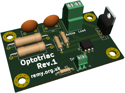
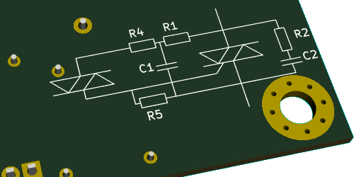
PCB markings
This is a PCB that at some point in the future I expect to re-use and rather than have to dig up the KiCAD design files it felt better to put the circuit diagram onto the back of the PCB itself. Resistor and capacitorR1/C1 is the snubber for the opto-triac and the resistor-capacitor pair R2/C2 is the snubber for the main power triac.
Resistor R4 is intended to avoid a dead-short to the power triac gate exceeding the opto-couplerITSM;
and resistor R5 is some sort of pull-down that the zero-crossing MOC3042 needs that the non-crossing MOC3021 does not, which I am guessing is needed by the former's zero-crossing detection functionality.
Doing away with synchronisation
As a simplification rather than active detection of a zero crossing using aMOC3021 optocoupler and using this to trigger activation pulse, the zero crossing MOC3042 is used and the triggering circuit simply outputs a pulse of slightly less than 20mS.
A pulse of 20mS is virtually guaranteed to contain exactly one zero crossing unless there is the utter bad luck of the pulse edge coinciding with an actual zero-crossing, but using a period slightly less than that of the AC wave-form means that if it does happen it will not happen again for a significant number of cycles, as the slight differences introduces a varying phase-shift.
As a result triggering can be done using a simple 555 oscillator circuit, and the one shown below had pulses of 15mS seperated by a space of 128mS, these periods being down to what components happened to be at close had rather than a specific target.