Capacitive dropper circuit
21 May 2023My last circuit project centered around the use of a capacitive voltage dropper as a way of getting low-voltage DC from main AC voltage without the use of a transformer, but this first attempt had many faults and the article itself ended up being a badly-explained mess. Here is a better job of explaining my understanding of a circuit that is more to the point of doing its core function and does not have the various flaws of the previous version. I cannot say I am entirely satisfied with my understanding and hence my explainations but this new version of the circuit itself seems faultless. It seemed better to leave my likely incorrect calculations in place and then remark on what I observed when the circuit was assembled and subsequently reworked.
Circuit design
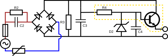
Compared to the previous circuit this one is intentionally minimalist, the main change being the removal of the zero-crossing detection and output triacs so that the circuit is purely for direct current power supply. The phase-shift that capacitive dropper introduce mean that they cannot be used with circuits that need to synchronise with mains frequency, so there was no point keeping any of the AC power control circuitry. The final stage voltage regulator has also been removed as this project is intended to be the first stage of a future power regulation project, and the zener diode is used as a voltage reference rather than having it shunt all the surplus voltage from the bridge rectifier.
Dropper and rectification
The main part of the circuit is the capacitive dropperC2 who'se reactance limits current flow, since with alternating current capacitors act like resistors and hence limit power transfer.
Assuming full-wave rectification with a frequency f and capacitance C the reactance X of a capacitor is given by the formulae below.
In Europe f is 50Hz so a capacitor valued at 2.2μF gives a reactance of around 1,447 ohms.
This capacitor will need to be rated to withstand peak mains voltage of 240√2 = 340 volts.
| X | = | 1 |
| 2 * π * f * C | ||
| = | 1 | |
| 2 * π * 50 * 2.2μ | ||
| ≈ | 1447Ω |
With 240 volt mains power this reactance limits the RMS current to 165mA although in practice voltage drops across other components in series will reduce the voltage drop across the capacitor and hence the current flow, but it provides a starting-point for other calculations.
The next component to consider is the smoothing capacitor C2 and in order to keep the ripples in the rectified DC output above 80 volts at all times a value of at least 6.35μF is required of the latter, although due to supply considerations a 10μF capacitor is used.
The high-value resistors R2 and R3 that are in parallel with capacitors C2 and C3 respectively are there for safety and they ensure that once mains power is disconnected these capacitors do not maintain a high-voltage charge.
Inrush current limitation
When power is first applied there is an effective dead-short acrossC2 and C3 which means the whole mains voltage is dropped across the fuse and a rectifier diode, and in order to avoid either blowing the fuse — or even worse tripping mains power breakers — this initial surge of mains current needs to be limited and one way of doing this is having a current-limiting resistance in series.
This can be a fixed-value resistor but a more efficent approach is a negative-coefficent thermister which provides an initial resistance that then reduces down to a fraction of its initial value.
In both cases the tricky part is deciding what component rating to use since the inrush current while large is also short-lived — of the order of a few AC cycles versus the maximum five seconds the 0312001.MXP fuse is rated to blow when subjected to twice its rated current.
A pessimistic calculation to limit inrush to 500mA with 240-volt mains (i.e. 340-volt peak) works out at needing 680Ω:
| R | = | 340v | = 680Ω |
| 500mA |
However a lot of material out there shows the use of under-100Ω resistors with a power rating of under 500mW, which I suspect is down to the short-lived nature of the inrush and the power drop when the circuit is in a steady-state. Since pretty much all the thermisters I could find have a “cold” resistance of 100Ω or less I suspect the choice of resistance is either focused more on steady-state losses rather than theoretical inrush, or the value is based on empirical experience. The notionally 50Ω thermister used in this circuit starts out at 62Ω but then drops to 20Ω immediately after power disconnection.
Emitter-follower circuit
Rather than using the zener diode to shunt surplus voltage an emitter-follower amplifier circuit is used, and this is marked by a dashed yellow box in the schematic above. The zener diodeD2 still regulates the output voltage but it is the NPN transistor that has to deal with the power dissipation caused by current draw at high voltages with the diode itself current-limited by R4.
With D2 having a reverse-drop of 75 volts R4 will have upto 265 volts across it, so to keep the zener diode's reverse-current below its rated maximum 13mA itr needs around 20kΩ of protection:
| R | = | 265v | = 20.4kΩ |
| 13mA |
A 22kΩ resistor was eventually used as the exact resistance is not really of any concern, so the selected component was based on cost rather than target value.
Inrush current is not a problem as the discharged smoothing capacitor C2 will bypass this entire section of the circult during the initial powerup surge, but the NPN transitor is rated to withstand C2 being charged up to full peak voltage.
The bypass capacitor C4 was included in the design to help smooth over small transcient changes in the voltage across the zener diode but in practice was left out of the final build of the circuit.
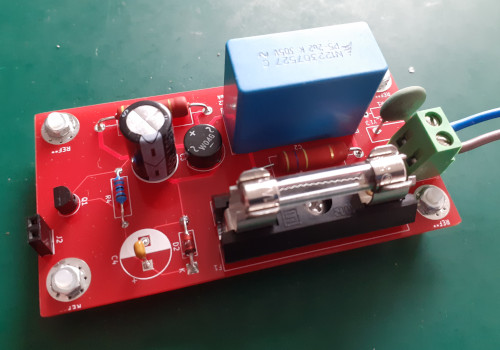
PCB fabrication
I had originally intended to make this revision of the circuit on prototyping board but in the end decided to make another PCB using JLCPCB, as the main cost is the shipping rather than fabrication itself and I already had one other PCB project in my backlog, and since the first revision PCB was a complete embaressment I felt the need for a respin. As with the previous version this was with JLCPCB but they are back to offering red PCBs which is my preferred way of indicating lead vs. lead-free.
Although the release candidate of KiCad 7 was available I felt it best to stick with KiCad 5 for this project. In more recent times I have tended to only opt for a PCB if I need to use surface-mount components but such projects are ones I prefer to avoid these days, and most of the project ideas have lined up are biased towards using discrete components rather than integrated circuit chips. I expect KiCad 7 to be very different to KiCad 5 and at the moment learning a new package is outside my bandwidth.
Practical use of the circuit
The voltage on the DC side of the bridge rectifier was circa 16 volts and I am at a loss as to why, since I thought the smoothing capacitor would reach something closer to the AC voltage in the absence of any real load but this is clearly not the case. The way that the dropper capacitor limits current clearly also cuts off the maximum rectifier output voltage but I have yet to come across any source that concisely explains what DC voltage is achievable. Since it was clear that the 75-volt rating of the zener diode would not be obtained it was replaced with a 6.2-volt rated one, and the circuit was tested with various output loads which are summerised in the table below.
| Component | Load | ||||||||
| None | 22kΩ | 11kΩ | 4.2kΩ | 2kΩ | 460Ω | 120Ω | 100Ω | 60Ω | |
| Smoothing capacitor (volts) | 6.67 | 6.50 | 6.68 | 6.67 | 6.64 | 6.54 | 6.07 | 5.98 | 5.47 |
| Zener diode (volts) | 6.55 | 6.50 | 6.56 | 6.58 | 6.54 | 6.45 | 6.02 | 6.91 | 5.44 |
| Base resistor (mV) | 37.3 | 36.9 | 37.1 | 37.0 | 36.7 | 35.1 | 28.3 | 26.92 | 21.3 |
| Output (volts) | 6.57 | 6.07 | 6.11 | 6.07 | 6.03 | 5.86 | 5.33 | 5.24 | 4.70 |
| Load current (mA) | n/a | 0.30 | 0.56 | 1.44 | 3.05 | 12.71 | 43.91 | 51.00 | 78.50 |
Within this circuit the voltage drop across the zener diode is also the transistor's base voltage and at least for the lower loads, the difference between the base voltage and the output voltage is around 0.55 volts which coincidentally is the same as the transistor's Vbe. The difference between the smoothing capacitor voltage drop and the output voltage also corresponds with VBE which makes me suspect that the transistor was saturated so it is acting like a switch rather than an amplifier. The voltage regulation part of the circuit is a shunt regulator which is basically potential-divider made using a resistor and a zener diode, as summerised in the schematic below.
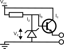
In this arrangment the resistor needs to be sized to allow for the minimum current draw Iz that the zener will operate with plus the base current required to allow the transistor to pass Ic to the output.
The transistor has a quoted minimum gain hfe of 40 so a base current Ib of 4mA should allow a collector current Ic of at least 160mA, although the data-sheet does hint of a potential gain of 200+ in some circumstances that don't seem far off the values for this circuit.
| Ib | = | Ic | ≈ | 4mA |
| hfe |
The zener diode's mimimum operating current Iz is 1mA so the resistor need to be sized so that the residual voltage drop would corresponds to 5mA, and here 16 volts is assumed as supply Vcc and from this the zener diode's 6.2 volts is subtracted.
| R | = | Vcc-Vz | ≈ | 10 volts | = | 2kΩ |
| Iz+Ib | 5mA |
In reality the voltage drop across this 2kΩ was 37mV which corresponds to 18.5μA which is not even close to the zener diode's specified minimum current, and this voltage drop was the same with a 22kΩ resistor. However when the zener diode was removed the 11kΩ load resistor in place got toasted as something close to 220 volts was being dropped across it, so while the measured values seemed odd at least qualitatively the circuit was behaving as designed.
List of components
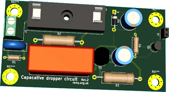
Below is a list of components that were used in populating the circuit board, which is a mix of items from existing stock and some bought in specially for the project so I would not be surprised if one or two of them have been discontinued by their manufacturer. The choice of components was partly influenced by which ones KiCad had footprints for, most notably being the fuse holder where the Schurter units were £2.82 each rather than the £0.32 that the cheapest alternative was. Not all of the pads on the PCB were populated so this table has gaps, and padsD2 & R4 list both the originally specified components and the ones that they were replaced with after some testing.
| Component | Manufacturer | Part number | PCB pad |
| 2.2μF X2 capacitor | Epcos | B32924C3225K000 |
C2 |
| 75v zener diode | ON Semiconductor | 1N5374BRLG |
D2 |
| 6.2v zener diode | Multicomp | 1N4735A |
|
| Terminal block | MC000034 |
J1 |
|
| Pin receptacle | 2212S-02SG-85 |
J2 |
|
| NPN transistor | MPSA44 |
Q1 |
|
| Bridge rectifier | W04G |
D1 |
|
| 10μF 450v capacitor | MCKSK450M100G17S |
C3 |
|
| 0.1μF capacitor | Vishay | K104K15X7RF53H5 |
C4 |
| pad not used | R1 |
||
| 470kΩ resistor | Vishay | PR03000204703JAC00 |
R2 |
R3 |
|||
| 2kΩ resistor | TE Connectivity | LR0204F2K0 |
R4 |
| 22kΩ resistor | Yageo | MF0207FTE52-22K |
|
| 50Ω NTC Thermistor | N10SP050M |
TH1 |
|
| Fuse holder | Schurter | 0031.8002 |
F1 |
| 1 Amp fuse | Littelfuse | 0312001.MXP |
n/a |
Below are the footprints used by each component since messing up the footprint selection was a major problem with the previous circuit. Note that the PCB pad numbers are a bit different since the PCB included an extra resistor not shown in the circuit design schematic. Finding the right footprint can be hard at times because their classification is not always obvious — for instance the thermistor footprint was listed under Varistors, and it was still a bit small for the thermistor used.
| Pad | PCB footprint |
F1 |
Fuseholder_Cylinder-6.3x32mm_Schurter_0031-8002_Horizontal_Open |
C2 |
C_Rect_L31.5mm_W13.0mm_P27.50mm_MKS4 |
C3 |
CP_Radial_D10.0mm_P5.00mm |
C4 |
|
R1 |
R_Axial_DIN0207_L6.3mm_D2.5mm_P10.16mm_Horizontal |
R2 |
R_Axial_DIN0617_L17.0mm_D6.0mm_P25.40mm_Horizontal |
R3 |
|
R4 |
Resistor_THT:R_Axial_DIN0309_L9.0mm_D3.2mm_P12.70mm_Horizontal |
J1 |
TerminalBlock_Phoenix_MKDS-1,5-2-5.08_1x02_P5.08mm_Horizontal |
J2 |
Connector_PinSocket_2.54mm:PinSocket_2x01_P2.54mm_Vertical |
D1 |
Diode_Bridge_Round_D9.8mm |
D2 |
D_DO-41_SOD81_P10.16mm_Horizontal |
TH1 |
RV_Disc_D12mm_W4.2mm_P7.5mm |
Q1 |
TO-92_Inline |
Remarks
The circuit was confirmed as being able to supply 80mA at five volts but the voltage drop fluctuates so much with current draw that further smoothing would be required for anything needing a consistent voltage, and all things considered it seems that using a transformer to step down the raw mains voltage is better as it makes a lot of complications go away. Capacative droppers are not really intended to deliver a lot of current and any circuit that I would want to supply from mains voltage is likely going to be a power control one that would use opto-coupliers for zero-crossing detection, the latter which did not work properly when mixed with captivate droppers. Factoring in the extra switching circuitry needed to obtain a consistent voltage and provide galvanic isolation seems like it would negate any size and cost advantage X2 capacitors have over a power transformer.
The project in itself was an interesting experience but like many other recent projects this one was mostly completed months ago and things got in the way of bringing it to a conclusion. This write-up could have been better since I don't fully understand the quantitative side but it is time to move onto other projects.