Triac circuit evaluation
26 December 2020This is a continuation of the hard-wired triac power control where due to circumstance I had to omit any real in-depth analysis of the circuit, and decided it better to complete and publish before the content got any more stale. With access to both the circuit and proper equipment in the same place I have now been able to do proper testing of the circuit, and the results are the subject of this update.
Phase signal testing
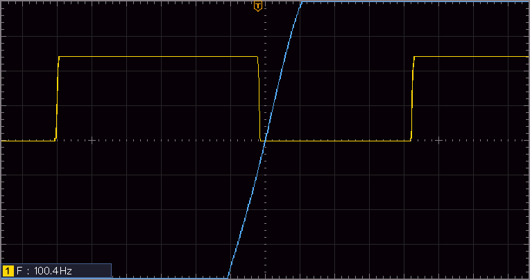
I did not want to connect the mains supply directly to my oscilloscope so instead the blue voltage trace was taken from the output of the isolation transformer on the switched power circuit. I suspect the truncation is caused by the circuitry that is connected to that side, but here the only thing that is relevent is the zero-crossing point rather than the shape or magnitude. The yellow trace is the phase signal, which consists of the output from theH11AA1 opto-coupler sub-circuit.
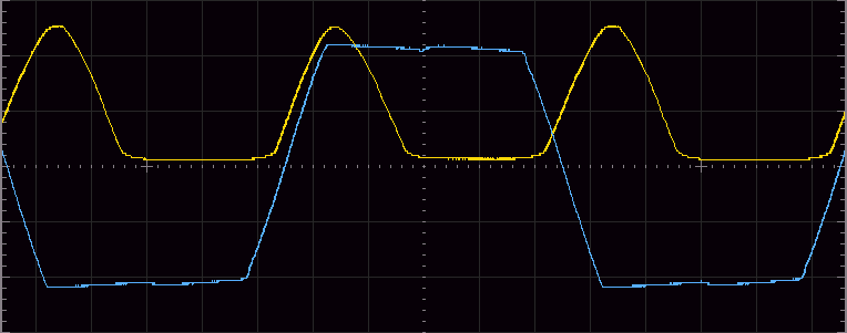
The phase signal seems to encompass the second derivative of the increasing magnitude part of the mains power sine wave — I am not sure why it takes this form and had I known in advance I would not have designed the circuit to feed this signal straight into the phase counter sub-system. I tied together the phase and enable signals to see what the input to the pulse-generation 555 timer, and as can be seen from the blue trace below has nice sharp rising and falling edges — this is nearer what I would have liked for the phase signal, and this is discussed later.
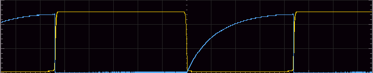
Zero-crossing alignment
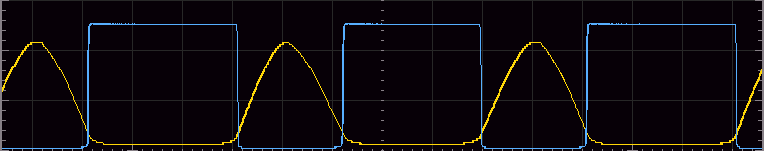
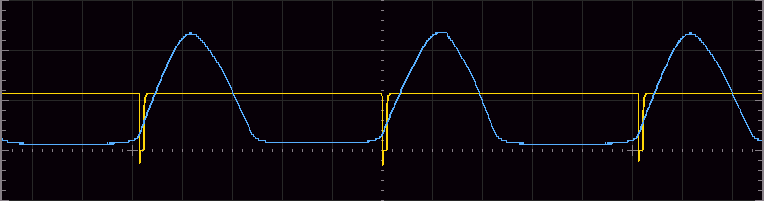
The phase signal is just an intermediary and what really matters is how the conversion of it to a square wave compares to the source power supply wave-form the former was itself derived from. In the plot below the blue trace is the input power supply and the yellow trace is what reaches the pulse-generation 555 timer, assuming the phase-counting circuitry enables it — for the purposes of this test the enable signal is tied to the phase signal.
An important factor with triac power control is how close the falling edge of the latter is to the AC crossing point and using the oscilloscope it leads the zero-crossing by 200μS — this is 1% of the 20mS a single cycle of 50Hz takes. Based on anecdotal information that a 786μS pulse is needed for reliable triac switch-on, which I note is of the same magnitude.
Phase signal pre-processing
Had I known what the phase signal would look like I would have pre-processed it in order to do two things: give it well-defined rising & falling edges, and give it a narrow pulse width. The simplest circuit I could come up with to do this is shown in the schematic below — it is active low because the 555 timer is triggered by a falling edge, and the rising edge would then trigger the phase counter increment so that there is not a race condition between the two.

One issue with this pre-processing circuit, at least on solder-less breadboard and can be seen in the oscilloscope trace below alongside the source phase signal, is that the output has a bit of negative-voltage noise and it is only half of the voltage rail level — the second of these is more critical but adding in an extra transistor should be able to fix it. In any case this is just a starting-point and will be part of a future project.
Enable counter testing
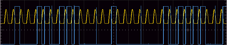
This sub-system is on a seperate circuit board so was mostly tested in isolation — I only connected the phase signal as a clock source. Although using a counter reference of0 resulted in the output always being low and f in it always being high, using values between these two resulted in unexpected behaviour.
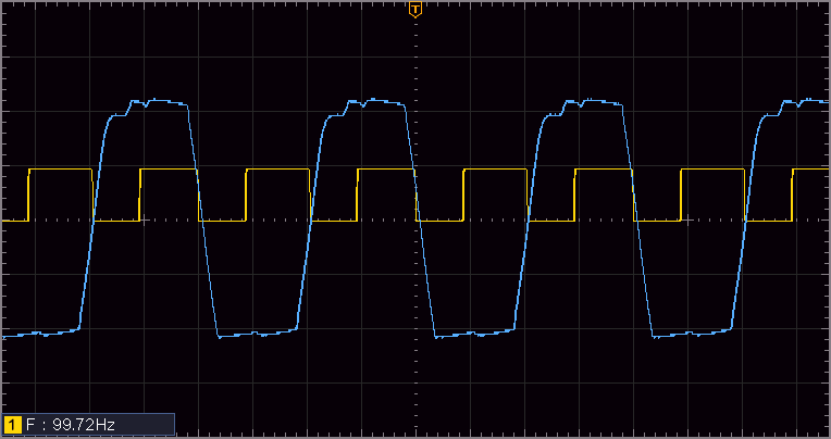
In the trace below yellow is the input clocking pulse and blue is the enable signal.
The latter should have batches of highs that are all of the same duration as well as batches of lows that are also all equal, but here both of them vary in width.
I decided to probe the SN74HC393N binary counter, where each output pin should be a frequency-dividier of the clock signal.
What I actually got was garbage, and I got the same results when I put in a clean square wave, so the chip is clearly dodgy.
I saw no point in testing the CD74HC85 binary comparator since it would be receiving duff values from the pulse counter.
The middle two output pins of the PCF8574 I/O expander were also shorted together, so I only tested reference values where these pins were the same — they are open-drain so flipping one of them would not cause any damage.
Supected issues with 555
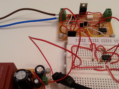
I suspected that there was an issue with the 555 chip on the triac circuit board, but rather than replacing it I decided to re-route the output of the transistor gate pair to an externally hosted chip as shown below — this is because I had been using the latter to experiment with astable timing in isolation and patch-wiring in the 555 trigger saved the need to unpack my desoldering equipment.
In astable operation once the threshold reaches two-thirds of Vcc, the output switches off which in turn grounds the open-drain discharge pin, but this does not happen while the trigger is still low; instead as seen in the oscilloscope trace below the capacitor remains charged until trigger is released. As a result the 555 chip acts as an inverting output buffer rather than a pulse emitter.
Putting a capacitor in front of the trigger input to shorten the input pulse fixed this issue. I did wonder whether I would then be better off replacing the astable oscillator with a Schmitt trigger, but I would most likley end up having to implement it with a 555 anyway as the off-the-shelf Schmitt triggers don't seem to have suitable specification tolerances. For some reason the fix did not solve the issue when I reworked the main circuit itself — maybe I also needed a resistor or a diode but a few electric shocks made me decide not to investigate further.
Remarks
Ideally much of the testing presented here would have been done during if not before I built the circuit, rather than several months later, but due to the circuit and oscilloscope being in different places until now I could not do that. Without access to an oscilloscope I would not have identified the short-comings of this power-control systems, although the design itself on the whole was sound given the knowledge I did have, and aside from reliability issues it basically worked. I am not sure if the faulty microchips were bad in first place or whether they sustained some of the damage during transit.For various reasons I decided that rather than reworking the circuit until it worked as expected I will wrap up this project and start over from scratch as a new project in the future — these are the passage of time, actually having all the required equipment in one place from the start, getting a few electric shocks from probing the circuit, and the overall difficulty in reworking already tightly-packed prototyping boards. With another round of lock-downs coming I need something to pass the time anyway.