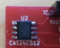
CAT24C512 EEPROM chip
01 March 2020In the past I have bought several EEPROM chips, with the longer-term view of using them to provide persistent state for a circuit, but the ON Semiconductor
CAT24C512 is the first that I got round to using in a circuit design as opposed to just reading the data-sheet.
However due to design issues the circuit was abandoned, although the underlying project itself is one I intend to revive at some point in the future.
In the mean-time the purpose of this article is a personal note of how to use the chip.
The PCB used as a breakout board is the same one that was repurposed for the recent article on RS232 line drivers, but the details are beyond the scope of this article. Although the microcontrollers that I am likely to use for the redesign have built-in data EEPROMs they tend to be relatively small, and the I2C interfaces of external chips are relatively predictable.
Chip pin-out
The KiCAD 5 symbol & footprint libraries do not include theCAT24C512 but they do include the CAT24C256 which has an identical pin-out and landing pattern — I am pretty sure the latter chip is a direct derivative of the former. The pin-out and symbol is shown in the table below.
| Address 1 | 1 |
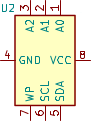 |
8 | Ground |
| Address 2 | 2 | 7 | Write protect | |
| Address 3 | 3 | 6 | I2C SCL | |
| Vcc | 4 | 5 | I2C SDA |
The write protect pin is active-high but here it is tied to ground there is no need for any write protection. The three address pins, which have internal pull-down resistors, set the low address I2C bytes as summerised below. The other pins are the two for the power supply pins, and the two for the I2C bus connection.
| 1 | 0 | 1 | 0 | A2 | A1 | A0 | R/W |
In the test circit all three address pins are tied high, so the I2C device address is 0xae for writes and 0xaf for reads.
Memory access
For demonstration purposes I will use commands for the Robot Electronics USB-ISS written to the device using my Python3 serial control script. I opted for the USB-ISS adapter rather than one of my own since the former is available off-the-shelf, although the commands below should be easy to translate into whatever is required by the controlling master. The command below sets up the adapter for 100kHz I2C, and if successful the two response bytes will be0xff then 0x00.
$ ./ttyTxRx3.py /dev/ttyACM0 2 5a 02 60 0
Flash writes
To write to flash the I2C transaction needs to include the two register bytes, and these indicate where in memory the first byte id written to — subsequent bytes in the transaction are written to subsequent addresses. The data-sheet refers to byte and sequence writes, but this distinction is meaningless in practice. The command below writes a sequence of 16 bytes starting at0x0080, and then a further 16 starting at address 0x0078 — these two memory ranges intentionally overlap.
$ ./ttyTxRx3.py /dev/ttyACM0 1 56 ae 0 80 f 11 12 13 14 15 16 17 18 19 1a 1b 1c 1d 1e 1f $ ./ttyTxRx3.py /dev/ttyACM0 1 56 ae 0 78 f 01 02 03 04 05 06 07 08 09 0a 0b 0c 0d 0e 0f
For the purpose of writes, memory is divided up into 512 pages of 128 bytes each. If a write operation crosses a page boundary, it wraps around to the beginning of the page rather than going into the next page. The data is committed to flash memory when the I2C write transaction stops, and while this committal to flash is in progress the device will not acknowledge transactions The data-sheet suggests using reads to poll whether the device is ready for further commands.
Flash reads
When reading the two-byte register address is optional, and if omitted reads will start from the last accessed address. Unlike with writes, read transactions can cross page boundaries and only wrap around when the end of memory is reached. The command below reads 16 bytes starting at address0x0070 and demonstrates this crossing of page boundaries.
$ ./ttyTxRx3.py /dev/ttyACM0 16 56 af 0 78 10 Sending 5 bytes.. Sent 5 Replies (16 expected): 1 2 3 4 5 6 7 8 11 12 13 14 15 16 17 18
16 bytes of data are returned and the values included in the snippet above.
The first 8 bytes are from the second write and the remaining 8 are from the first write, due to reads not wrapping at page boundaries like writes do.
On a new chip each address is initially set to 0xff.