PCA9655E breakout
04 February 2018While I was doing the reflow for the PCA9671 expander breakout I also used the same PCB board to mount an ON Semiconductor
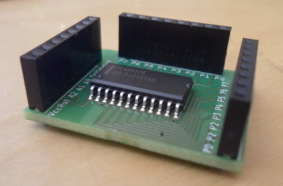
PCA9655E (Farnell 2464421) since aside from having an interrupt pin rather than a reset, the pin-outs are virtually identical. As it turned out this I/O expander is functionally identical to the TCA9535, while having the higher total current draw tolerance and address range of the PCA9671. As a result this article will highlight the differences.

The PCA9655E is register-based where all I2C transactions, including pin reads & writes, use an internal 8-byte address. The 16 input/output pins are divided into two 8-bit ports, which operate independently. Each pin can sink 50mA with a combined ground current limit of 600mA, although there is a recommended limit of 25mA per pin.
Usage
I2C communication of the expander makes use of the same register addresses as theTCA9535, so the sub-sections below will only cover the difference. One nice feature is the ability to use a multi-byte transaction to read/write more than one register at once — I did not check at the time whether the TCA9535 also allows this — which is particularly useful as it allows one transaction to deal with all 16 pins over the two ports.
Address pins
Like thePCA9671, the PCA9655E expander uses the I2C SDA & SCL lines as input for the device address selection pins in addition to Vcc and Ground. I am not exactly sure how it works, but my suspicion it is an elimination process based on comparing when the pins change state, assuming they change at all. There is quite likley coordination between manufacturers as the address table in the data-sheet has the same mapping as that in the PCA9671 data-sheet, and is replicated below:
| Address pins | I2C address | |||
| A2 | A1 | A0 | Write | Read |
Gnd |
Scl |
Gnd |
0x20 | 0x21 |
Gnd |
Scl |
Vcc |
0x22 | 0x23 |
Gnd |
Sda |
Gnd |
0x24 | 0x25 |
Gnd |
Sda |
Vcc |
0x26 | 0x27 |
Vcc |
Scl |
Gnd |
0x28 | 0x29 |
Vcc |
Scl |
Vcc |
0x2a | 0x2b |
Vcc |
Sda |
Gnd |
0x2c | 0x2d |
Vcc |
Sda |
Vcc |
0x2e | 0x2f |
Gnd |
Scl |
Gnd |
0x30 | 0x31 |
Gnd |
Scl |
Vcc |
0x32 | 0x33 |
Gnd |
Sda |
Gnd |
0x34 | 0x35 |
Gnd |
Sda |
Vcc |
0x36 | 0x37 |
Vcc |
Scl |
Gnd |
0x38 | 0x39 |
Vcc |
Scl |
Vcc |
0x3a | 0x3b |
Vcc |
Sda |
Gnd |
0x3c | 0x3d |
Vcc |
Sda |
Vcc |
0x3e | 0x3f |
Gnd | Gnd | Gnd |
0x40 | 0x41 |
Gnd | Gnd | Vcc |
0x42 | 0x43 |
Gnd | Vcc | Gnd |
0x44 | 0x45 |
Gnd | Vcc | Vcc |
0x46 | 0x47 |
Vcc | Gnd | Gnd |
0x48 | 0x49 |
Vcc | Gnd | Vcc |
0x4a | 0x4b |
Vcc | Vcc | Gnd |
0x4c | 0x4d |
Vcc | Vcc | Vcc |
0x4e | 0x4f |
Gnd |
Gnd |
Scl |
0x50 | 0x51 |
Gnd |
Gnd |
Sda |
0x52 | 0x53 |
Gnd |
Vcc |
Scl |
0x54 | 0x55 |
Gnd |
Vcc |
Sda |
0x56 | 0x57 |
Vcc |
Gnd |
Scl |
0x58 | 0x59 |
Vcc |
Gnd |
Sda |
0x5a | 0x5b |
Vcc |
Vcc |
Scl |
0x5c | 0x5d |
Vcc |
Vcc |
Sda |
0x5e | 0x5f |
Scl |
Scl |
Gnd |
0xa0 | 0xa1 |
Scl |
Scl |
Vcc |
0xa2 | 0xa3 |
Scl |
Sda |
Gnd |
0xa4 | 0xa5 |
Scl |
Sda |
Vcc |
0xa6 | 0xa7 |
Sda |
Scl |
Gnd |
0xa8 | 0xa9 |
Sda |
Scl |
Vcc |
0xaa | 0xab |
Sda |
Sda |
Gnd |
0xac | 0xad |
Sda |
Sda |
Vcc |
0xae | 0xaf |
Scl |
Scl |
Scl |
0xb0 | 0xb1 |
Scl |
Scl |
Sda |
0xb2 | 0xb3 |
Scl |
Sda |
Scl |
0xb4 | 0xb5 |
Scl |
Sda |
Sda |
0xb6 | 0xb7 |
Sda |
Scl |
Scl |
0xb8 | 0xb9 |
Sda |
Scl |
Sda |
0xba | 0xbb |
Sda |
Sda |
Scl |
0xbc | 0xbd |
Sda |
Sda |
Sda |
0xbe | 0xbf |
Scl |
Gnd |
Gnd |
0xc0 | 0xc1 |
Scl |
Gnd |
Vcc |
0xc2 | 0xc3 |
Scl |
Vcc |
Gnd |
0xc4 | 0xc5 |
Scl |
Vcc |
Vcc |
0xc6 | 0xc7 |
Sda |
Gnd |
Gnd |
0xc8 | 0xc9 |
Sda |
Gnd |
Vcc |
0xca | 0xcb |
Sda |
Vcc |
Gnd |
0xcc | 0xcd |
Sda |
Vcc |
Vcc |
0xce | 0xcf |
Scl |
Gnd |
Scl |
0xe0 | 0xe1 |
Scl |
Gnd |
Sda |
0xe2 | 0xe3 |
Scl |
Vcc |
Scl |
0xe4 | 0xe5 |
Scl |
Vcc |
Sda |
0xe6 | 0xe7 |
Sda |
Gnd |
Scl |
0xe8 | 0xe9 |
Sda |
Gnd |
Sda |
0xea | 0xeb |
Sda |
Vcc |
Scl |
0xec | 0xed |
Sda |
Vcc |
Sda |
0xee | 0xef |
Addresses ranges 0x00-0x1e, 0xd0-0xde, and 0xf0-0xfe are not used. Some of these correspond to I2C reserved addresses which ought not be used anyway.
Interrupts
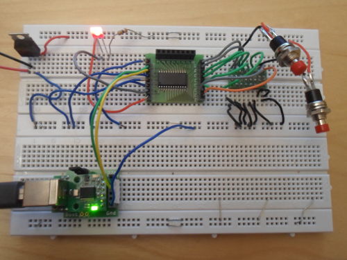
Due to a PCB design error I was not able to verify the expected interrupt behaviour of thePCA9671, but since no such error exist with this breakout board, I did a quick test of the interrupt pin using the setup shown below. The interrupt pin is active-low open-drain, and it resets either when the port with the changed pin is read or the pins return to the pre-interrupt state.

I am not exactly sure how it resolves the reset when pins on both have changed but only one port is read, so I would be inclined to read both ports with a two-byte read:
./ttyTxRx.py /dev/ttyACM0 2 55 41 00 2
Remarks
While it was a nice discovery that the command set was identical to an I/O expander I had tried out in the past, I find the command-orientated ones that use register addresses to be a bit of a pain. The MicrochipMCP23017 seemed to include 1 or 2 fringe options purely because there was the spare capacity, but the others I have tried are not quite so pathological. Personally I prefer the zero-configuration nature of the 8-bit PCF8574 and 16-bit PCA9671, the latter being physically identical to the expander this article details.