Darlington array measurments
07 January 2018This article is a follow-up to my Darlington transistor array write-up, where I will compare the theoretical and actual values of power related to the constituent components. This was originally going to be point of discussion for a circuit board that would use the Darlington array PCB, along with other daughter-boards such as the TCA9535 breakout board, but this large-scale project was one I decided to abandon before all the daughter-boards PCBs were delivered. I spun the content off to a seperate article because the issues are of interest in their own right.
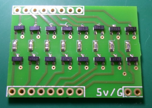
The Darlington array board was conceived with the row driver of my LED matrix display in mind, although it also doubled up being a secondary foray into SMD circuits. The idea was to allow low-current positive-logic to switch on and off a high-current parallel interface, and was made in mind with the amount of space that parallel resisitor-transistor sub-circuits take up. It made sense as a lot of the circuits I ended up building were basically grid-orientated power supplies, even if the architecture is less clear in my 7/8-segment LED displays citcuits.
Test circuit
For testing purposes I wired up one of the eight transistor pairs as shown in the schematic below, with a resistor between the PNP collector and ground acting as the electrical load. Originally I wanted to intentionally draw 300mA as this was roughly the original design target current, but by far the smallest resistor I had was 20Ω which would have resulted in a draw around the 200mA. This clearly exceeded its rated value of 250mW and as a result was getting hot fairly quickly, so I also tested using 40Ω (two 20Ω in series) & 380Ω for comparison purposes. I then measured various voltages which are listed in the table, alongside the expected values I used when calculating the original electrical values.
| Exp. | 380Ω | 20Ω | 40Ω | |
| Vec | 620mV | 10mV | 120mV | 60mV |
| Veb | 1.2V | 766mV | 762mV | 790mV |
| R | 3.5V | 4.14V | 3.83V | 4.0V |
| Load | n/a | 4.9V | 4.54V | 4.68V |
| Vce | 300mV | 4.6mV | 4.4mV | 4.5mV |
| Vcc | 5V | 4.93V | 4.5V | 4.77V |
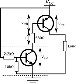
I suspect the power supply was struggling with 20Ω & 40Ω as the power drop Vcc across the entire circuit was significantly below the nominal 5 volts, and Vec varied a bit. Given that quoted data-sheet voltages are maximums some variance between expected & measured values is to be expected, but the voltage drop Vceacross the current-sinking NPN transistor is well below the expected value — it is basically negligible, meaning the drop across the control-current limiting resistor R is 15-20% above expectation. Therefore I should have opted for 800Ω rather than 680Ω to target a control current of 5mA.
Low NPN voltage drops
Looking at the graphs in the NPN transistor's data-sheet rather than the tables, I think the quoted maximum 0.3 volts for Vce is a mis-print and that it should really be 0.03 volts. However 4 volts across 680Ω ought to be about 6mA, which according to the graph should be a Vce of 20mV, which is still a lot higher than the measured 4.5mV, but nevetheless 20mV looks like a saner maximum value. I have noticed in the past that voltage drops across NPN transistors tend to be far from what data-sheets claim they should be, and within a 5 volt circuit I would regard anything in the 5-20mV range to be negligable. I expect the voltage drop to be low due to the amount of current also being low, particularly as this transistor has a power rating well above what it is actually supplying, but the graph specifically shows the collector current range that is of interest in this circuit.As a result of a 5-20mV potential difference, I would have assumed 3.8 volts across resistor R, which with a target 5mA would require 760Ω rather than the actual 680Ω. Not vastly difference in the grand scale of things, and saving a few milliwatts in the intra-transistor signal line is insignificant compared to quarter-to-half amp each array output is specified to provide, but component selection has to start somewhere.