PCF8574 I/O Expander
13 March 2021The Texas Instruments
PCF8574 is pretty much the first I/O Expander chip and first I2C device I ever used and it is a contender for the chip I have used the most when creating circuits.
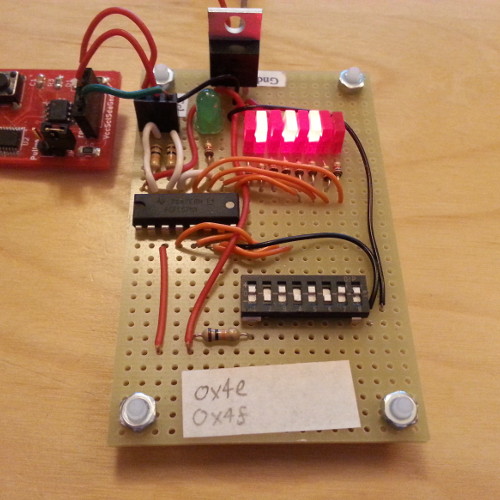
Being zero-configuration I have often used it for test purposes and finally decided to make a permanent test circuit based around the chip; this demonstration circuit is shown below.
Since I had not used the chip for some time and did not have the data-sheets at hand I decided to write a mini-article with all the relevant information so that I would not need to go digging for it again.
Chip pinning
The chip pinning for the PCF8574 is summetised in the table below, where Ax are address pins and Px are input/output pins.
On chip reset all of the latter pins are set to high-impedance and hence input rather than output.
| Vcc | SDA | SCL | Int | P7 | P6 | P5 | P4 |
| 16 | 15 | 14 | 13 | 12 | 11 | 10 | 9 |
| 1 | 2 | 3 | 4 | 5 | 6 | 7 | 8 |
| A0 | A1 | A2 | P0 | P1 | P2 | P3 | Gnd |
Upon an I2C write pins that have a high written become high-impedance whereas those with a low written will sink current; upon a subsequent read pins sinking current will always read as low whereas the hi-impedence pins will read high or low dependent on external driving.
The interrupt pin like the input/output pins is open-drain, and is active-low so it will conduct when the input value that would be read is different to the previous I2C transaction; this means an interrupt will be deasserted if the input reverts to the previous value.
The I2C address is set by the A0 thru A2 pins as per the table below.
| Address pins | I2C | |||
A0 |
A1 |
A2 |
Read |
Write |
0 |
0 |
0 |
0x41 |
0x40 |
1 |
0 |
0 |
0x43 |
0x42 |
0 |
1 |
0 |
0x45 |
0x44 |
1 |
1 |
0 |
0x47 |
0x46 |
0 |
0 |
1 |
0x49 |
0x48 |
1 |
0 |
1 |
0x4b |
0x4a |
0 |
1 |
1 |
0x4d |
0x4c |
1 |
1 |
1 |
0x4f |
0x4e |
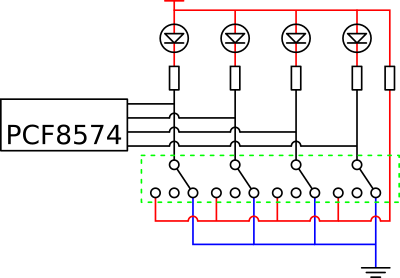
Test circuit schematic
The essential parts of the test circuit is summerised in the simplified schmatic shown below — the idea is that pins used for output should have the associated tri-state DIP switch set to open-circuit, but the wiring is such that there are no ill-effects such as a low-resistance path between power rails if this is not done.