Solid-state AC control
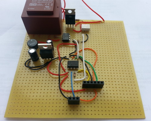
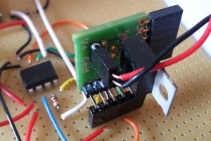
05 September 2020One thing I was not sure with my previous relay-based AC switches is how quickly they could actually switch, so before long I decided to look at solid-state high-power switching using thyristors, although before I got round to building an actual test circuit I had turned my attention to triac devices instead. This circuit is a prototype solid-state switch that uses the latter, although unlike my relay-based switches it was built in prototyping board and it is shown below. Although the previous relays were designed to switch 240-volt mains, this is the first circuit I have built which requires it for proper operation, and when I started I was not even sure if it was safe to use such voltages on prototyping board.
Background
Over the summer while over in the UK I had got back into hot-plate reflow soldering, for which I had got hold of a cheap mains-powered hot-plate, and before long I was thinking up circuits that could be used to control it — firstly thermocouple sensors and then power relays. I was never really happy with the mechanical relay solutions so it is not surprise I ended up looking at solid-state power electronics, and since I now having access to me usual equipment and component stocks I felt it was time for experimental circuit prototyping. I am not sure if I would actually build a fully-automatic hot-plate for reflowing, but in any case I was not going to stop developing all the building blocks for creating one.
Design parameters
Joop Brokking's YouTube video was clear an inspiration, although my preferred approach would not involve modding of the hot-plate itself. The goal with this circuit is having solid-state power control of an AC device that is rated at several amperes, since that is the current that a typical hot-plate would actually draw. For safety reasons although I would use components rated for this load, I would not attempt to test this load on prototyping boards. I also wanted to have the control circuit powered from the AC mains rather than requiring a separate power supply, something that was a part of my second abandoned relay-based circuit.Thyristor vs. triac devices
A triac (triode for AC) is functionally two thyristors in opposite directions attached together, the idea being that they are in turn triggered to account for the swapping of voltage polarity in alternating current. The tricky thing with the triggering of triac devices is that the voltage supplied to the gate has to take account of the current polarity of the AC supply, and that means the gate cannot just be directly controlled by a direct-current signal of the usual ground and Vcc levels for low and high. As a first-pass I was going to use thyristors and accept only being able to use the positive half of the AC power cycle, but I never got as far as designing such a circuit before getting my head around how to use triac devices instead.DC power sub-circuit
For this project I decided to have the control circuitry powered from the AC supply since it is more convenient than having to rely on a separate power source. The DC power sub-circuit consists of a step-down transformer to reduce the 240VAC to 12VAC, a bridge rectifier together with a smoothing capacitor to convert this into DC, and finally a linear regulator to provide the required 5-volt DC supply. All this is summerised in the schematic below:

Transformer
The transformer is a VigortronixVTX-121-3015-212 isolation transformer that steps down 230 volts into two 12-volt windings, which I think I originally bought since it was the cheapest transformer I could find that stepped mains voltage down to something suitable for 5-volt linear power regulators. The transformer is rated at 1.5VA and a current draw of 62mA, the latter of which I think is per secondary winding (i.e. per output).
One output winding is used for control circuit power whereas the other is used for phase detection of the input mains — I did not read up on whether it is possible to wire up these windings in parallel to get double the current.
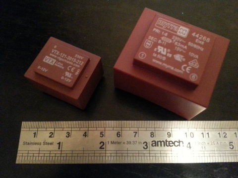
One thing I noticed is that transformers for stepping down mains voltage to something below 24 volts get big & expensive pretty quickly.
The picture above shows the 62mA Vigortronix VTX-121-3015-212which cost £2.18+VAT and was just under 9cm2 of PCB real-estate, and the Myrra 44268 667mA which came in costing £5.60+VAT and taking up 21cm2.
The former is just about bearable but the latter is a real pain — the size of the Myrra was instrumental in why I decided not to fabricate the power relay I had designed that made use of it
Rectifier smoothing capacitor
The transformer's rating of 65mA is the limiting factor for how much power is available for the control circuitry, so there is no technical value in specifying anything higher than this for the power regulation circuitry. The drop-out voltage of the Texas InstrumentsLM2940x with this current draw is safely below 100mV across the entire temperature range, and with a peak of 12√2 volts coming off the bridge rectifier this means the linear regulator can cope with a ripple of about 11.87 volts.
As shown by the calculation below — the formulae is in an earlier article — this means a smoothing capacitor of at least 55μF is needed:
| C = | 65mA | = 55μF |
| 2 * 50Hz * 11.87V |
In practice I used a 100μF capacitor because it was the cheapest one I could find that was both above 55μF and had the required voltage rating, and using it meant the regulator could actually supply 118mA without dropping out, leaving aside issues with this exceeding the transformer's specifications.
Linear voltage regulator
I opted for the Texas InstrumentsLM2940CT-5.0 due to its low drop-out voltage, with the express aim of requiring a smaller smoothing capacitor across the connection with the bridge rectifier, although as it happened this would not end up being a limiting factor.
Linear rectifiers are notoriously inefficient since they need to dissipate as heat the power resulting from the difference between the actual import voltage and the intended output voltage. If the input and output voltages are Vinput & Voutput respectively and the current draw is Iload the amount of power that needs dissipating is given by the following formulae.
The power dissipation is a major problem if the difference between supply & output voltages — and/or the current draw — is big.
(Vinput - Voutput) * Iload
Within this circuit the power draw is the practically negligable amount required by the main controller, and even if it required anything close to what the DC supply sub-circuit is rated for, it is still negligable compared to the currents the AC switching sub-circuit is specified to handle. In the past I never really paid much attention to the power supply but this circuit is contemporary with me looking into switched-mode power supplies — however the power requirements of the control sub-circuit meant the latter was never a serious consideration for this project.
Regulator by-pass capacitor
In the past I have normally omitted the decoupling capacitor across the regulator output but in this case doing so resulted in it supplying 7 volts rather than the specified 5 volts — although not high enough to damage the chips within the low-voltage part of the circuitry it was high enough to stop things working properly. I suspect that the input voltage being raw rectifier output with a lot of ripple rather than something clean like a 9-volt D-cell may have played a part. Most if not all the regulators I have used in the past only recommended a capacitor but the data-sheet for theLM2940CT explicitly requires one of at least 22μF — maybe this is due to its ultra-low dropout voltage compared to regulators I have used previously.
AC switching sub-circuit
The mains AC switching is done by a Ween SemiconductorsBT136-600D/DG,127 therac as the main “switch” and in turn this is triggered by an ON Semiconductor MOC3021M optocoupler which provides isolation between the high-voltage and low-voltage parts of the circuit, and this setup is summarised in the schematic below.
Using a therac-output optocoupler to trigger a triac means that the control circuit does not need to concern itself with which way the AC cycle is polarised, as well as providing isolation from the low-voltage control part of the circuit.
A more sophisticated design would include snubbing via resistor/diode configurations but for this experimental project I left them out.

One thing to watch out for is that the polarity of the triac matters.
On the prototyping board itself I had the main terminals swapped so that the direction of current flow for the gate connection was opposite of what it needed to be, and as a result it was not getting triggered.
I am unsure whether this is an intentional thing with the MOC3021M, as some stuff I have read indicates that triacs should still trigger in such circumstances.
Waveform chopping
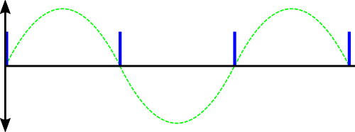
Once a thyristor/theac is switched on it does not switch off until the AC reverses, hence why it is better regarded as a trigger rather than a gate as with transistors, and the effect it has on power supplied is summarised in the graph below. Only supplying power for part of the alternating-current cycle provides a lot of control over how much power is provided to the downstream devices the power circuit is controlling.
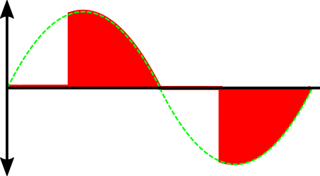
Actual power supplied is the area between the curve and the x-axis, which can be calculated via integration. Power control can be done either by chopping up individual AC cycles as shown above, or by cutting out entire cycles and/or half-cycles. Although the original plan was to do the former and chop up individual wave-forms, in the end the firmware was written to do the latter.
Zero-crossing vs. non-zero
Triac-output photo-couplers are advertised either ZC (zero-crossing) and NZC (non zero crossing) and this indicates whether the triac can be triggered at any arbitrary point, or whether there is a little extra circuitry that only allows it on a voltage flip. The reason for only triggering while the voltage is low is that it avoids a huge amount of high-frequency noise, some of which gets emitted as RF radiation and this often has regulatory consequences in addition to other problems. The down-side is that it means only cutting off complete half-waves which limits the power-control ability of the circuit. In practice with circuits where there is a digital controller that has synchronisation with the AC power supply, there is no real advantage of using a zero-cross because the controller itself can achieve the same effect of only triggering during voltage cross-over.AC synchronisation sub-circuit
The controlling circuit needs to know when to trigger the AC switching circuit, and this means having a synchronisation signal from the mains power supply itself. I felt it best to have as little as possible connected directly to the mains supply, so the synchronization is done from the low-voltage side of the transformer using the circuit below. I had originally intended to do phase-detection directly from the mains AC and hence why an opto-isolated transistor was specified for safety reasons, but opto-isolatioon still seemed the best way to deal with the voltage difference between the transformer output and the control circuit itself.

Phase signal
Although not to scale the graph below gives an indication of when the phase signal is asserted. The LED within the opto-isolated transistor package has a typical forward voltage of 1.15 volts so for 12VAC (peak voltage of 12√2 ≈ 16.97) this means it will be lit 0.0215π either side of a zero crossing, which gives a pulse width of 430μS.
Trigger timing
Since the AC synchronisation sub-circuit uses an LED-based opto-coupler the phase signal is actually asserted before the zero-crossing occurs, so ideally the controller needs to hold back on triggering the triacs in the switching sub-circuit until as close to the actual zero-crossing as possible, which in theory should be right in the middle of the phase signal pulse. Adjusting this trigger offset to achieve this is one instance that gpsim is very useful when writing the firmware, as the phase signal can be simulated as a periodic digital signal and it can be shown graphically alongside the resulting trigger signal as shown in the screenshot snippet below. This helps take guess-work and calculations out of writing firmware delay loops.
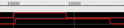
Ideally the delay and pulse width should be trimmed based on testing of the actual circuit with an oscilloscope, but since I don't have an oscilloscope at hand I was not able to do this, and as a result do not know how close the simulated signals match the physical circuit. What I do know from trial-and-error is that the notional 786μS pulse width that generated the trace above under simulation is close to the mimimum width required that would reliably trigger the triac on the physical hardware.
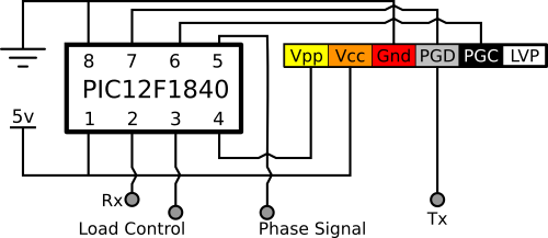
Main control sub-circuit
A MicrochipPIC12F1840 is used as the main controller due to familiarity with the microcontroller sub-family, although I think the stock I used is actually from 2017 or 2018 — if I needed to order in the chips I likley would have gone for the PIC16F1823 instead due to the larger number of pins.
The schematic below shows the connections it has with both the other sub-circuits and the outside world.
The RS232 Tx and in-circuit serial programming PGC functions have to share the same pin but this is a minor issue.
RS232 connection
RS232 is my go-to protocol when I want to provide an external interface for a circuit and as a result I include it on this circuit. While in practice only the receive functionality is likely to be used, and this is why I put this pin in the middle of the header, it is my standard practice to include the transmit line as well because having an out-bound channel has come in handy in the past when debugging. For this circuit most obvious use would be to provide mains frequency information. In the past I have often also included an I2C interface but in practice have rarely made use of such interfaces.In-Circuit serial programming
The times I have decided to rely on either swapping a chip out into a programming seat or making use of a programming clip have more often than not been varying levels of pain, so for this circuit I have done my now-preferred things of including an in-circuit serial programming header. This takes up a surprisingly large portion of the whole circuit but the pay-off in reduced hassle during firmware development is both immediate and huge. The colour-coding of the programming header reflects the colours of the ribbon cable my PICkit programmer happened to come with.
Control firmware
The firmware for this circuit is within my Bitbucket repository and like other projects in there it may or may not be updated in the future. Much of the actual firmware development was done using gpsim rather than running on the actual circuit since this is one project where the abstraction provided by gpsim were very close to what the microcontroller would actually see. I tend not to dwell much on firmware these days since within experimental circuits such as this they are just a means to an end.Use of assembly
Ever since I put together my thoughts on PIC assembly programming I have basically concluded that PIC microcontrollers should only ever be programmed using assembly. While it was helpful using C when figuring things out, the PIC architecture is one where the abstractions made result in a disproportionate loss of control with little gain to show for it, and something like my recent thermocouple control would simply not be feasible. All the design decisions that would push me towards using C rather than assembly are also the ones that would push me towards using ARM instead of PIC. On the plus side assembly programming has a certain satisfaction to it, and this is why I have not simply abandoned the PIC architecture and move over entirely to ARM.Chopping within vs. between waves
Although keeping entire half-waves intact avoids generating a lot of high-frequency noise the firmware takes this approach for a rather different reason — not having to really care what the actual AC mains frequency is. With control limited to half-waves the firmware just needs an interrupt handler triggered by the phase detection to check a counter and from there it can basically go to sleep, whereas chopping up the half-waves needs careful timing that has to overlap with the communications routines. While being limited to half-waves is not suitable for lighting due to resulting flicker, it is fine for the heater-control that is the notional design use-case for this circuit.Remarks
Originally I did not include a voltage regulator output capacitor so testing of the board was done with the 5 volts being supplied via the programming header from a known-good source. It was only at the very end that I ordered in and added the required capacitor since the design goal of not needing a separate DC power supply was secondary to the experimentation with triac-based power control, but it did mean that I could consider the board to be a complete success rather than a partial one.
With the equipment I have at hand I cannot evaluate the circuit much beyond seeing what I qualitatively expected successful operation to be, whereas ideally I would want to at least see what the output wave-form looks like on an oscilloscope. So far this is only the third circuit I have built that one would have been really useful so I am not sure if the €500+ price tag for a half-decent one is worth it, but I get the feeling it is an investment decision I will have to make before long.